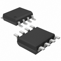
MAX5015ESA+ Maxim Integrated Products, MAX5015ESA+ Datasheet - Page 12

MAX5015ESA+
Manufacturer Part Number
MAX5015ESA+
Description
IC CNTRLR PWM CRNT MD 8-SOIC
Manufacturer
Maxim Integrated Products
Datasheet
1.MAX5015ESA.pdf
(14 pages)
Specifications of MAX5015ESA+
Pwm Type
Current Mode
Number Of Outputs
1
Frequency - Max
275kHz
Duty Cycle
50%
Voltage - Supply
18 V ~ 110 V
Buck
No
Boost
No
Flyback
No
Inverting
No
Doubler
No
Divider
No
Cuk
No
Isolated
Yes
Operating Temperature
-40°C ~ 85°C
Package / Case
8-SOIC (3.9mm Width)
Frequency-max
275kHz
Duty Cycle (max)
50 %
Output Current
1000 mA
Mounting Style
SMD/SMT
Switching Frequency
275 KHz
Maximum Operating Temperature
+ 85 C
Minimum Operating Temperature
- 40 C
Synchronous Pin
No
Topology
Flyback, Forward
Lead Free Status / RoHS Status
Lead free / RoHS Compliant
6) Choose R
7) Choose the inductor value so that the peak ripple
Current-Mode PWM Controllers with Integrated
Startup Circuit for Isolated Power Supplies
12
ing equation to calculate the tertiary winding turns
ratio:
where:
V
V
V
V
design example).
N
N
Choose N
where:
V
voltage (0.465V).
N
example).
I
this example).
current (LIR) in the inductor is between 10% and
20% of the maximum output current.
OUTMAX
ILim
DDMIN
DDMAX
IN_MIN
IN_MAX
P
T
S
______________________________________________________________________________________
/N
is the number of turns of the tertiary winding.
is the number of turns of the primary winding.
P
is the current-sense comparator trip threshold
R
is the secondary side turns ratio (5/14 in this
is the minimum V
SENSE
L
is the minimum input voltage (36V).
R
is the maximum V
is the maximum input voltage (72V in this
SENSE
is the maximum DC output current (10A in
T
SENSE
≥
= 6.
2
13 7
5 33
×
(
36
.
V
V
V
LIR
≤
.
DDMIN
DDMAX
OUT
according to the following equation:
≤
V
V
N
N
≤
×
IN_MIN
IN_MAX
×
P
14
S
N
1
5
275
+
4
T
×
0 465
+
×
V
+
≤
1 2 . I
.
≤
1 2 10
0 7
D
kHz I
0 7
N
7 14
V
.
.
)
.
ILIM
DD
T
.
×
×
DD
V
×
×
≤
×
(
OUTMAX
×
1
N
supply voltage (13V).
N
36 7
-
P
supply voltage (36V).
72
OUTMAX
D
P
=
.
≤
MIN
109
N
×
T
14
)
≤
m
Ω
All connections carrying pulsed currents must be very
short, be as wide as possible, and have a ground plane
as a return path. The inductance of these connections
must be kept to a minimum due to the high di/dt of the
currents in high-frequency switching power converters.
Current loops must be analyzed in any layout pro-
posed, and the internal area kept to a minimum to
reduce radiated EMI. Ground planes must be kept as
intact as possible.
TRANSISTOR COUNT: 589
PROCESS: BiCMOS
8) The size and ESR of the output filter capacitor deter-
where V
age drop (0.5V) and LIR is the ratio of inductor rip-
ple current to DC output current.
mine the output ripple. Choose a capacitor with a
low ESR to yield the required ripple voltage.
Use the following equations to calculate the peak-to-
peak output ripple:
where:
V
V
capacitive ripple. Calculate the ESR ripple and
capacitive ripple as follows:
V
V
RIPPLE
RIPPLE,ESR
RIPPLE,ESR
RIPPLE,C
V
RIPPLE
D
is the combined RMS output ripple due to
L
is the output Schottky diode forward volt-
= I
Layout Recommendations
≥
= I
, the ESR ripple, and V
RIPPLE
0 4 275
( )
.
=
5 5
RIPPLE
.
×
V
RIPPLE ESR
×
2
/(2 x π x 275kHz x C
(
1 0 198
kHz
x ESR
-
.
Chip Information
,
×
10
)
A
+
V
=
RIPPLE C
2
4 01
.
µ
RIPPLE,C
H
,
OUT
)
, the


