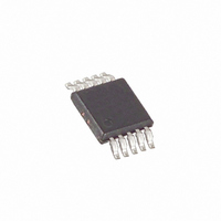
MAX669EUB+ Maxim Integrated Products, MAX669EUB+ Datasheet - Page 15

MAX669EUB+
Manufacturer Part Number
MAX669EUB+
Description
IC PWM BST FLYBCK ISO CM 10UMAX
Manufacturer
Maxim Integrated Products
Datasheet
1.MAX669EUB.pdf
(18 pages)
Specifications of MAX669EUB+
Pwm Type
Current Mode
Number Of Outputs
1
Frequency - Max
575kHz
Duty Cycle
94%
Voltage - Supply
1.8 V ~ 28 V
Buck
No
Boost
Yes
Flyback
Yes
Inverting
No
Doubler
No
Divider
No
Cuk
No
Isolated
Yes
Operating Temperature
-40°C ~ 85°C
Package / Case
10-MSOP, Micro10™, 10-uMAX, 10-uSOP
Frequency-max
575kHz
Output Current
6 A
Switching Frequency
500 KHz
Operating Supply Voltage
1.8 V to 28 V
Supply Current
0.22 mA
Maximum Operating Temperature
+ 85 C
Minimum Operating Temperature
- 40 C
Mounting Style
SMD/SMT
Output Voltage
3 V to 28 V
Duty Cycle (max)
94 %
Synchronous Pin
Yes
Topology
Boost, Flyback
Lead Free Status / RoHS Status
Lead free / RoHS Compliant
not be adequate for low output voltage ripple. Since
output ripple in boost DC-DC designs is dominated by
capacitor equivalent series resistance (ESR), a capaci-
tance value 2 or 3 times larger than C
cally needed. Low-ESR types must be used. Output
ripple due to ESR is:
The input capacitor (C
current peaks drawn from the input supply and reduces
noise injection. The value of C
by the source impedance of the input supply. High
source impedance requires high input capacitance,
particularly as the input voltage falls. Since step-up DC-
DC converters act as “constant-power” loads to their
input supply, input current rises as input voltage falls.
Consequently, in low-input-voltage designs, increasing
C
percentage points to conversion efficiency. A good
starting point is to use the same capacitance value for
C
In addition to C
capacitors are also required with the MAX668/MAX669.
Bypass REF to GND with 0.22µF or more. Bypass LDO
to GND with 1µF or more. And bypass V
0.1µF or more. All bypass capacitors should be located
as close to their respective pins as possible.
Output ripple voltage due to C
stability by introducing a left half-plane zero. A small
capacitor connected from FB to GND forms a pole with
the feedback resistance that cancels the ESR zero. The
optimum compensation value is:
where R2 and R3 are the feedback resistors (Figures 2,
3, 4, and 5). If the calculated value for C
non-standard capacitance value, values from 0.5C
1.5C
In non-bootstrapped configurations (Figures 4 and 5),
the MAX668 can start up with any combination of out-
put load and input voltage at which it can operate when
already started. In other words, there are no special
limitations to start-up in non-bootstrapped circuits.
IN
IN
C
FB
as for C
and/or lowering its ESR can add as many as five
FB
will also provide sufficient compensation.
C
V
OUT
OUT
RIPPLE(ESR)
x
Applications Information
.
IN
(R2 x R3) / (R2 + R3)
______________________________________________________________________________________
and C
IN
ESR
= I
) in boost designs reduces the
OUT
LPEAK
COUT
Compensation Capacitor
Starting Under Load
, three ceramic bypass
IN
OUT
x ESR
is largely determined
Bypass Capacitors
ESR affects loop
1.8V to 28V Input, PWM Step-Up
OUT(MIN)
Input Capacitor
COUT
CC
FB
to GND with
results in a
is typi-
FB
to
In bootstrapped configurations with the MAX668 or
MAX669, there may be circumstances where full load
current can only be applied after the circuit has started
and the output is near its set value. As the input voltage
drops, this limitation becomes more severe. This char-
acteristic of all bootstrapped designs occurs when the
MOSFET gate is not fully driven until the output voltage
rises. This is problematic because a heavily loaded out-
put cannot rise until the MOSFET has low on-resis-
tance. In such situations, low-threshold FETs (V
V
Operating Characteristics section shows plots of start-
up voltage versus load current for a typical boot-
strapped design.
Due to high current levels and fast switching waveforms
that radiate noise, proper PC board layout is essential.
Protect sensitive analog grounds by using a star ground
configuration. Minimize ground noise by connecting
GND, PGND, the input bypass-capacitor ground lead,
and the output-filter ground lead to a single point (star
ground configuration). Also, minimize trace lengths to
reduce stray capacitance, trace resistance, and radiat-
ed noise. The trace between the external gain-setting
resistors and the FB pin must be extremely short, as
must the trace between GND and PGND.
Figure 3 shows the MAX669 operating in a low-voltage
boost application. The MAX669 is configured in the
bootstrapped mode to improve low input voltage per-
formance. The IRF7401 N-channel MOSFET was select-
ed for Q1 in this application because of its very low
0.7V gate threshold voltage (V
a 5V output at greater than 2A of output current and
operates with input voltages as low as 1.8V. Efficiency
is typically in the 85% to 90% range.
Figure 5 shows the MAX668 operating in a 5V to 12V
boost application. This circuit provides output currents
of greater than 1A at a typical efficiency of 92%. The
MAX668 is operated in non-bootstrapped mode to mini-
mize the input supply current. This achieves maximum
light-load efficiency. If input voltages below 5V are
used, the IC should be operated in bootstrapped mode
to achieve best low-voltage performance.
Figure 6 shows the MAX668 in a SEPIC (single-ended
primary inductance converter) configuration. This con-
figuration is useful when the input voltage can be either
IN(MIN)
Controllers in µMAX
) are the most effective solution. The Typical
4-Cell to 5V SEPIC Power Supply
Layout Considerations
Low-Voltage Boost Circuit
Application Circuits
GS
12V Boost Application
). This circuit provides
TH
15
<


