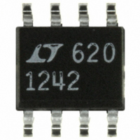
LT1242CS8 Linear Technology, LT1242CS8 Datasheet - Page 9

LT1242CS8
Manufacturer Part Number
LT1242CS8
Description
IC PWM CURRENT MODE HI-SPD 8SOIC
Manufacturer
Linear Technology
Datasheet
1.LT1245IN8.pdf
(16 pages)
Specifications of LT1242CS8
Pwm Type
Current Mode
Number Of Outputs
1
Frequency - Max
500kHz
Duty Cycle
96%
Voltage - Supply
11 V ~ 25 V
Buck
Yes
Boost
No
Flyback
No
Inverting
No
Doubler
No
Divider
No
Cuk
No
Isolated
Yes
Operating Temperature
0°C ~ 100°C
Package / Case
8-SOIC (3.9mm Width)
Frequency-max
500kHz
Lead Free Status / RoHS Status
Contains lead / RoHS non-compliant
Available stocks
Company
Part Number
Manufacturer
Quantity
Price
Company:
Part Number:
LT1242CS8
Manufacturer:
LT
Quantity:
10 000
Part Number:
LT1242CS8
Manufacturer:
LT/凌特
Quantity:
20 000
Part Number:
LT1242CS8#PBF
Manufacturer:
LINEAR/凌特
Quantity:
20 000
Part Number:
LT1242CS8#TRPBF
Manufacturer:
LINEAR/凌特
Quantity:
20 000
A
Current Sense Comparator and PWM Latch
LT1241 series devices are current mode controllers.
Under normal operating conditions the output (Pin 6) is
turned on at the start of every oscillator cycle, coincident
with the rising edge of the oscillator waveform. The output
is then turned off when the current reaches a threshold
level proportional to the error voltage at the output of the
error amplifier. Once the output is turned off it is latched
off until the start of the next cycle. The peak current is thus
proportional to the error voltage and is controlled on a
cycle by cycle basis. The peak switch current is normally
sensed by placing a sense resistor in the source lead of the
output MOSFET. This resistor converts the switch current
to a voltage that can be fed into the current sense input. For
normal operating conditions the peak inductor current,
which is equal to the peak switch current, will be equal to:
During fault conditions the maximum threshold voltage at
the input of the current sense comparator is limited by the
internal 1V clamp at the inverting input. The peak switch
current will be equal to:
In certain applications, such as high power regulators, it
may be desirable to limit the maximum threshold voltage
to less than 1V in order to limit the power dissipated in the
sense resistor or to limit the short-circuit current of the
regulator circuit. This can be accomplished by clamping
the output of the error amplifier. A voltage level of
approximately 1.4V at the output of the error amplifier will
give a threshold voltage of 0V. A voltage level of approxi-
mately 4.4V at the output of the error amplifier will give
a threshold level of 1V. Between 1.4V and 4.4V the
threshold voltage will change by a factor of one-third of the
PPLICATI
I
I
PK
PK MAX
V
PIN
3
1
1 0
R
R
O
S
S
1 4
V
U
V
S
I FOR ATIO
U
W
U
change in the error amplifier output voltage. The threshold
voltage will be 0.333V for an error amplifier voltage of
2.4V. To reduce the maximum current sense threshold to
less than 1V the error amplifier output should be clamped
to less than 4.4V.
Blanking
A unique feature of the LT1241 series devices is the built-
in blanking circuit at the output of the current sense
comparator. A common problem with current mode
PWM circuits is erratic operation due to noise at the
current sense input. The primary cause of noise problems
is the leading edge current spike due to transformer
interwinding capacitance and diode reverse recovery
time. This current spike can prematurely trip the current
sense comparator causing an instability in the regulator
circuit. A filter at the current sense input is normally
required to eliminate this instability.
This filter will in turn slow down the current sense loop.
A slow current sense loop will increase the minimum pulse
width which will increase the short-circuit current in an
overload condition. The LT1241 series devices blank (lock
out) the signal at the output of the current sense compara-
tor for a fixed amount of time after the switch is turned on.
This effectively prevents the PWM latch from tripping due
to the leading edge current spike.
The blanking time will be a function of the voltage at the
feedback pin (Pin 2). The blanking time will be 100ns for
normal operating conditions (V
time goes to zero as the feedback pin is pulled to 0V. This
means that the blanking time will be minimized during
start-up and also during an output short-circuit fault. This
blanking circuit eliminates the need for an input filter at the
current sense input except in extreme cases. Eliminating
the filter allows the current sense loop to operate with
minimum delays, reducing peak currents during fault
conditions.
FB
LT1241 Series
= 2.5V). The blanking
9


