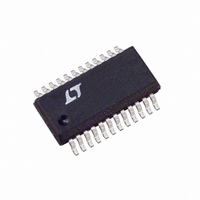
LTC3722EGN-2 Linear Technology, LTC3722EGN-2 Datasheet - Page 7

LTC3722EGN-2
Manufacturer Part Number
LTC3722EGN-2
Description
IC CTRLR PWM VOLTAGE-MODE 24SSOP
Manufacturer
Linear Technology
Datasheet
1.LTC3722EGN-1PBF.pdf
(28 pages)
Specifications of LTC3722EGN-2
Pwm Type
Voltage Mode, Full Bridge
Number Of Outputs
1
Frequency - Max
1MHz
Duty Cycle
98.5%
Voltage - Supply
3.8 V ~ 10.3 V
Buck
No
Boost
No
Flyback
No
Inverting
No
Doubler
No
Divider
Yes
Cuk
No
Isolated
Yes
Operating Temperature
-40°C ~ 85°C
Package / Case
24-SSOP
Frequency-max
1MHz
Lead Free Status / RoHS Status
Contains lead / RoHS non-compliant
Available stocks
Company
Part Number
Manufacturer
Quantity
Price
Part Number:
LTC3722EGN-2
Manufacturer:
LINEAR/凌特
Quantity:
20 000
pin FuncTions
SYNC (Pin 1/Pin 1): Synchronization Input/Output for the
Oscillator. The input threshold for SYNC is approximately
1.9V, making it compatible with both CMOS and TTL logic.
Terminate SYNC with a 5.1k resistor to GND.
DPRG (Pin 2/Pin 5): Programming Input for Default Zero
Voltage Transition (ZVS) Delay. Connect a resistor from
DPRG to V
A, B, C, D. The nominal voltage on DPRG is 2V.
RAMP (NA/Pin 2): Input to Phase Modulator Comparator
for LTC3722-2 only. The voltage on RAMP is internally
level shifted by 650mV.
CS (Pin 3/Pin 3): Input to Phase Modulator for the
LTC3722-1. Input to pulse-by-pulse and overload current
limit comparators, output of slope compensation circuitry.
The pulse by pulse comparator has a nominal 300mV
threshold, while the overload comparator has a nominal
650mV threshold.
COMP (Pin 4/Pin 4): Error Amplifier Output, Inverting
Input to Phase Modulator.
R
ing. Use a 10k to 100k resistor to program from 40ns to
310ns of leading edge blanking of the current sense signal
on CS for the LTC3722-1. A ±1% tolerance resistor is
recommended. The LTC3722-2 has a fixed blanking time
of approximately 80ns.
FB (Pin 6/Pin 6): Error Amplifier Inverting Input. This is
the voltage feedback input for the LTC3722. The nominal
regulation voltage at FB is 1.204V.
SS (Pin 7/Pin 7): Soft-Start/Restart Delay Circuitry Timing
Capacitor. A capacitor from SS to GND provides a controlled
ramp of the current command (LTC3722-1), or duty cycle
(LTC3722-2). During overload conditions SS is discharged
to ground initiating a soft-start cycle.
NC (Pin 8/Pin 8): No Connection. Tie this pin to GND.
PDLY (Pin 9/Pin 9): Passive Leg Delay Circuit Input. PDLY
is connected through a voltage divider to the left leg of
the bridge in adaptive ZVS mode. In fixed ZVS mode, a
voltage between 0V and 2.5V on PDLY, programs a fixed
ZVS delay time for the passive leg transition.
LEB
(Pin 5/NA): Timing Resistor for Leading Edge Blank-
REF
to set the maximum turn on delay for outputs
(LTC3722-1/LTC3722-2)
SBUS (Pin 10/Pin 10): Line Voltage Sense Input. SBUS is
connected to the main DC voltage feed by a resistive volt-
age divider when using adaptive ZVS control. The voltage
divider is designed to produce 1.5V on SBUS at nominal
V
configured for fixed mode ZVS control.
ADLY (Pin 11/Pin 11): Active Leg Delay Circuit Input. ADLY
is connected through a voltage divider to the right leg of
the bridge in adaptive ZVS mode. In fixed ZVS mode, a
voltage between 0V and 2.5V on ADLY, programs a fixed
ZVS delay time for the active leg transition.
UVLO (Pin 12/Pin 12): Input to Program System Turn-
On and Turn-Off Voltages. The nominal threshold of the
UVLO comparator is 5V. UVLO is connected to the main
DC system feed through a resistor divider. When the
UVLO threshold is exceeded, the LTC3722-1/LTC3722-2
commences a soft-start cycle and a 10µA (nominal) cur-
rent is fed out of UVLO to program the desired amount of
system hysteresis. The hysteresis level can be adjusted
by changing the resistance of the divider.
SPRG (Pin 13/Pin 13): A resistor is connected between
SPRG and GND to set the turn-off delay for the synchronous
rectifier driver outputs (OUTE and OUTF). The nominal
voltage on SPRG is 2V.
V
is capable of supplying up to 18mA to external circuitry.
V
capacitor.
OUTF (Pin 15/Pin 15): 50mA Driver for Synchronous
Rectifier Associated with OUTB and OUTC.
OUTE (Pin 16/Pin 16): 50mA Driver for Synchronous
Rectifier Associated with OUTA and OUTD.
OUTD (Pin 17/Pin 17): 50mA Driver for Low Side of the
Full Bridge Active Leg.
V
LTC3722-1/LTC3722-2 and 10.25V Shunt Regulator.
The chip is enabled after V
allow the V
UVLO comparator threshold is exceeded. Once the V
shunt regulator has turned on, V
6V (typ) and maintain operation.
IN
REF
REF
CC
. If SBUS is tied to V
(Pin 18/Pin 18): Supply Voltage Input to the
(Pin 14/Pin 14): Output of the 5V Reference. V
should be decoupled to GND with a 1µF ceramic
CC
LTC3722-1/LTC3722-2
shunt regulator to conduct current and the
REF
, the LTC3722-1/LTC3722-2 is
CC
has risen high enough to
CC
can drop to as low as
372212fa
REF
CC


