IR3624MTRPBF International Rectifier, IR3624MTRPBF Datasheet - Page 13
IR3624MTRPBF
Manufacturer Part Number
IR3624MTRPBF
Description
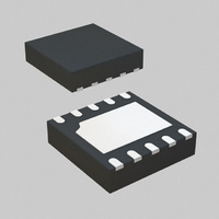
IC CTRLR PWM SYNC BUCK 10-MLPD
Manufacturer
International Rectifier
Datasheet
1.IR3624MPBF.pdf
(21 pages)
Specifications of IR3624MTRPBF
Package / Case
10-MLPD
Voltage - Supply
4.5 V ~ 14 V
Frequency-max
660kHz
Operating Temperature
-40°C ~ 125°C
Number Of Outputs
1
Duty Cycle
71%
Pwm Type
Voltage Mode
Buck
Yes
Boost
No
Flyback
No
Inverting
No
Doubler
No
Divider
No
Cuk
No
Isolated
No
Frequency
600kHz
Supply Voltage Range
4.5V To 14V
Digital Ic Case Style
MLPD
No. Of Pins
10
Operating Temperature Range
-40°C To +125°C
Termination Type
SMD
Input Voltage Primary Min
5V
Rohs Compliant
Yes
Filter Terminals
SMD
Control Mode
Voltage
Controller Type
PWM
Package
10-Lead MLPD
Circuit
Sync PWM Controller
Vcc (min)
4.0
Vcc (max)
14
Vout (min)
0.6
Vout (max)
Vcc * 0.71
Iout (a)
10
Switch Freq (khz)
Internal 600kHz
Pbf
PbF Option Available
Lead Free Status / RoHS Status
Lead free / RoHS Compliant
Other names
IR3624MPBFTR
Available stocks
Company
Part Number
Manufacturer
Quantity
Price

Part Number:
IR3624MTRPBF
Manufacturer:
IR
Quantity:
20 000


Power MOSFET Selection
The IR3624 uses two N-Channel MOSFETs. The
selections criteria to meet power transfer
requirements is based on maximum drain-source
voltage (V
maximum output current, On-resistance R
and thermal management.
The MOSFET must have a maximum operating
voltage (V
voltage (V
The gate drive requirement is almost the same
for both MOSFETs. Logic-level transistor can be
used and caution should be taken with devices at
very low V
complementary MOSFET, which results a shoot-
through current.
The total power dissipation for MOSFETs
includes conduction and switching losses. For
the Buck converter the average inductor current
is equal to the DC load current. The conduction
loss is defined as:
The R
considered for the worst case operation. This is
typically given in the MOSFET data sheet.
Ensure that the conduction losses and switching
losses do not exceed the package ratings or
violate the overall thermal budget.
For this design, IRF8910 is a good choice. The
device provides two N-MOSFETs in a compact
SO-8 package.
The IRF8910 has the following data:
The conduction losses will be: P
The switching loss is more difficult to calculate,
even though the switching transition is well
understood. The reason is the effect of the
parasitic components and switching times during
the switching procedures such as turn-on / turn-
off delays and rise and fall times. The control
MOSFET contributes to the majority of the
ϑ
P
P
V
R
cond
cond
ds
ds
=
(
=
on
R
=
=
)
20
ds(on)
=
(upper
(lower
DS(on)
V
13
temperatur
,
I
.
in
4
d
DSS
gs
DSS
).
m
=
switch)
switch)
temperature dependency should be
10
Ω
to prevent undesired turn-on of the
), gate-source drive voltage (V
) exceeding the maximum input
@
A
V
e
gs
=
=
=
I
I
load
dependency
2
load
2
10
∗
V
∗
R
R
ds(on)
ds(on)
∗
∗
(1
D
con
∗
−
ϑ
=0.724W
D)
∗
ϑ
DS(on)
gs
),
switching losses in synchronous Buck converter.
The synchronous MOSFET turns on under zero
voltage conditions, therefore, the turn on losses
for synchronous MOSFET can be neglected.
With a linear approximation, the total switching
loss can be expressed as:
Where:
V
t
t
T = Switching period
I
The switching time waveforms is shown in
figure12.
From IRF8910 data sheet:
tr = 10ns
tf = 4.1ns
These values are taken under a certain condition
test. For more details please refer to the IRF8910
data sheet.
By using equation (10), we can calculate the
switching losses. P
r
f
load
= Fall time
= Rise time
ds(off)
90%
10%
= Load current
V
V
GS
Fig. 12: switching time waveforms
P
DS
sw
= Drain to source voltage at the off time
t
d
=
(ON)
V
ds
2
(
off
)
*
t
r
T
+
sw
t
t
=0.37W
r
f
*
I
load
t
IR3624MPBF
d
(OFF)
-
- -
(10)
t
f
13
Related parts for IR3624MTRPBF
Image
Part Number
Description
Manufacturer
Datasheet
Request
R

Part Number:
Description:
SCHOTTKY RECTIFIER
Manufacturer:
International Rectifier Corp.
Datasheet:
Part Number:
Description:
SCHOTTKY RECTIFIER
Manufacturer:
International Rectifier Corp.
Datasheet:
Part Number:
Description:
SCHOTTKY RECTIFIER
Manufacturer:
International Rectifier Corp.
Datasheet:
Part Number:
Description:
SCHOTTKY RECTIFIER
Manufacturer:
International Rectifier Corp.
Datasheet:
Part Number:
Description:
SCHOTTKY RECTIFIER
Manufacturer:
International Rectifier Corp.
Datasheet:
Part Number:
Description:
SCHOTTKY RECTIFIER
Manufacturer:
International Rectifier Corp.
Datasheet:
Part Number:
Description:
SCHOTTKY RECTIFIER
Manufacturer:
International Rectifier Corp.
Datasheet:
Part Number:
Description:
SCHOTTKY RECTIFIER
Manufacturer:
International Rectifier Corp.
Datasheet:
Part Number:
Description:
SCHOTTKY RECTIFIER
Manufacturer:
International Rectifier Corp.
Datasheet:
Part Number:
Description:
SCHOTTKY RECTIFIER
Manufacturer:
International Rectifier Corp.
Datasheet:
Part Number:
Description:
SCHOTTKY RECTIFIER
Manufacturer:
International Rectifier Corp.
Datasheet:
Part Number:
Description:
SCHOTTKY RECTIFIER
Manufacturer:
International Rectifier Corp.
Datasheet:
Part Number:
Description:
SCHOTTKY RECTIFIER
Manufacturer:
International Rectifier Corp.
Datasheet:
Part Number:
Description:
SCHOTTKY RECTIFIER
Manufacturer:
International Rectifier Corp.
Datasheet:
Part Number:
Description:
SCHOTTKY RECTIFIER
Manufacturer:
International Rectifier Corp.
Datasheet: