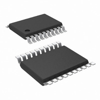
LM5035BMHX/NOPB National Semiconductor, LM5035BMHX/NOPB Datasheet - Page 17

LM5035BMHX/NOPB
Manufacturer Part Number
LM5035BMHX/NOPB
Description
IC CTRLR BRIDGE PWM 105V 20TSSOP
Manufacturer
National Semiconductor
Series
PowerWise®r
Datasheet
1.LM5035BMHNOPB.pdf
(28 pages)
Specifications of LM5035BMHX/NOPB
Pwm Type
Voltage Mode
Number Of Outputs
1
Frequency - Max
1MHz
Voltage - Supply
13 V ~ 105 V
Buck
No
Boost
No
Flyback
No
Inverting
No
Doubler
No
Divider
No
Cuk
No
Isolated
Yes
Operating Temperature
-40°C ~ 125°C
Package / Case
20-TSSOP Exposed Pad, 20-eTSSOP, 20-HTSSOP
Frequency-max
2MHz
Lead Free Status / RoHS Status
Lead free / RoHS Compliant
Duty Cycle
-
Other names
LM5035BMHX
Available stocks
Company
Part Number
Manufacturer
Quantity
Price
Company:
Part Number:
LM5035BMHX/NOPB
Manufacturer:
NS/TI
Quantity:
800
Applications Information
The following information is intended to provide guidelines for
the power supply designer using the LM5035B.
VIN
The voltage applied to the VIN pin, which may be the same
as the system voltage applied to the power transformer’s pri-
mary (V
into VIN depends primarily on the gate charge provided to the
output drivers, the switching frequency, and any external
loads on the VCC and REF pins. It is recommended the filter
shown in
occur at the input supply. This is particularly important when
VIN is operated close to the maximum operating rating of the
LM5035B.
When power is applied to VIN and the UVLO pin voltage is
greater than 0.4V, the VCC regulator is enabled and supplies
current into an external capacitor connected to the VCC pin.
When the voltage on the VCC pin reaches the regulation point
of 7.6V, the voltage reference (REF) is enabled. The refer-
ence regulation set point is 5V. The HO, LO, SR1 and SR2
outputs are enabled when the two bias regulators reach their
set point and the UVLO pin potential is greater than 1.25V. In
typical applications, an auxiliary transformer winding is con-
nected through a diode to the VCC pin. This winding must
raise the VCC voltage above 8.3V to shut off the internal start-
up regulator.
After the outputs are enabled and the external VCC supply
voltage has begun supplying power to the IC, the current into
VIN drops below 1 mA. VIN should remain at a voltage equal
to or above the VCC voltage to avoid reverse current through
protection diodes.
PWR
Figure 6
FIGURE 6. Input Transient Protection
), can vary in the range of 13 to 105V. The current
be used to suppress transients which may
FIGURE 7. Start-Up Regulator for V
30091322
17
FOR APPLICATIONS >100V
For applications where the system input voltage exceeds
100V or the IC power dissipation is of concern, the LM5035B
can be powered from an external start-up regulator as shown
in
should be connected together, which allows the LM5035B to
be operated below 13V. The voltage at the VCC pin must be
greater than 8.3V yet not exceed 15V. An auxiliary winding
can be used to reduce the power dissipation in the external
regulator once the power converter is active. The NPN base-
emitter reverse breakdown voltage, which can be as low as
5V for some transistors, should be considered when selecting
the transistor.
CURRENT SENSE
The CS pin needs to receive an input signal representative of
the transformer’s primary current, either from a current sense
transformer or from a resistor in series with the source of the
LO switch, as shown in
the sensed current creates a ramping voltage across R1, and
the R
C
and the ground connection from the current sense trans-
former, or R1, should be a dedicated track to the AGND pin.
The current sense components must provide greater than
0.25V at the CS pin when an over-current condition exists.
F
Figure
should be located as close to the LM5035B as possible,
F
/C
F
PWR
7. In this configuration, the VIN and the VCC pins
filter suppresses noise and transients. R1, R
>100V
Figure 8
30091323
and
Figure
9. In both cases,
www.national.com
F
and


