TL594CDR2G ON Semiconductor, TL594CDR2G Datasheet
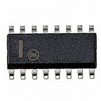
IC PWM CTRLR SWITCHMODE 16-SOIC

TL594CDR2G

Manufacturer Part Number
TL594CDR2G
Description
IC PWM CTRLR SWITCHMODE 16-SOIC
Manufacturer
ON Semiconductor
Series
SWITCHMODE™r
Datasheet

Specifications of TL594CDR2G

Pwm Type
Voltage Mode
Number Of Outputs
1
Frequency - Max
300kHz
Duty Cycle
50%
Voltage - Supply
7 V ~ 40 V
Buck
Yes
Boost
No
Flyback
No
Inverting
No
Doubler
No
Divider
No
Cuk
No
Isolated
No
Operating Temperature
-40°C ~ 85°C
Package / Case
16-SOIC (3.9mm Width)
Frequency-max
300kHz
Number Of Pwm Outputs
2
On/off Pin
No
Adjustable Output
No
Topology
Push-Pull
Switching Freq
300KHz
Operating Supply Voltage (max)
40V
Output Current
500mA
Synchronous Pin
No
Rise Time
100ns
Fall Time
40ns
Operating Temperature Classification
Industrial
Mounting
Surface Mount
Pin Count
16
Package Type
SOIC
Switching Frequency
300 KHz
Duty Cycle (max)
48 %
Operating Supply Voltage
15 V
Maximum Operating Temperature
+ 85 C
Minimum Operating Temperature
- 40 C
Mounting Style
SMD/SMT
Lead Free Status / RoHS Status
Lead free / RoHS Compliant

Available stocks

Company
Part Number
Manufacturer
Quantity
Price
Part Number:
TL594CDR2G
Manufacturer:
ON Semiconductor
Quantity:
53
Part Number:
TL594CDR2G
Manufacturer:
ON/安森美
Quantity:
20 000
TL594
Precision Switchmode
Pulse Width Modulation
Control Circuit
circuit designed primarily for Switchmode power supply control.
Features
Maximum ratings are those values beyond which device damage can occur.
Maximum ratings applied to the device are individual stress limit values (not
normal operating conditions) and are not valid simultaneously. If these limits are
exceeded, device functional operation is not implied, damage may occur and
reliability may be affected.
1. Maximum thermal limits must be observed.
*For additional information on our Pb−Free strategy and soldering details, please
© Semiconductor Components Industries, LLC, 2005
November, 2005 − Rev. 5
MAXIMUM RATINGS
download the ON Semiconductor Soldering and Mounting Techniques
Reference Manual, SOLDERRM/D.
Power Supply Voltage
Collector Output Voltage
Collector Output Current
Amplifier Input Voltage Range
Power Dissipation @ T
Thermal Resistance
Operating Junction Temperature
Storage Temperature Range
Operating Ambient Temperature Range
Derating Ambient Temperature
The TL594 is a fixed frequency, pulse width modulation control
Complete Pulse Width Modulation Control Circuitry
On−Chip Oscillator with Master or Slave Operation
On−Chip Error Amplifiers
On−Chip 5.0 V Reference, 1.5% Accuracy
Adjustable Deadtime Control
Uncommitted Output Transistors Rated to 500 mA Source or Sink
Output Control for Push−Pull or Single−Ended Operation
Undervoltage Lockout
Pb−Free Packages are Available*
(Each Transistor) (Note 1)
Junction−to−Ambient (PDIP)
Junction−to−Air (TSSOP)
Junction−to−Ambient (SOIC)
TL594CD, CN, CDTB
Rating
A
≤ 45°C
Symbol
I
C1
R
V
V
V
T
V
P
T
T
T
C1
, I
qJA
stg
CC
C2
IR
A
A
D
J
C2
,
−55 to +125
−0.3 to +42
−40 to 85
Value
1000
500
140
135
125
42
42
80
45
1
°C/W
Unit
mW
mA
°C
°C
°C
°C
V
V
V
See detailed ordering and shipping information in the package
dimensions section on page 10 of this data sheet.
1
Compen/PWN
1
Comp Input
(Note: Microdot may be in either location)
Deadtime
1
Noninv
Control
Ground
Input
Input
A
WL, L
YY, Y
WW, W = Work Week
G or G
ORDERING INFORMATION
Inv
C1
C
R
T
T
PIN CONNECTIONS
1
2
3
4
5
6
7
8
DTB SUFFIX
http://onsemi.com
CASE 751B
CASE 948F
TSSOP−16
CASE 648
N SUFFIX
D SUFFIX
PDIP−16
≈ 0.1 V
SO−16
+
Error
Amp
= Assembly Location
= Wafer Lot
= Year
= Pb−Free Package
Oscillator
1
(Top View)
Q1
Publication Order Number:
V
CC
16
2 Error
1
16
1
5.0 V
Amp
REF
16
+
Q2
1
DIAGRAMS
AWLYYWWG
TL594CDG
MARKING
AWLYWW
TL594CN
16
15
14
13
12
11
10
9
ALYWG
4DTB
TL59
V
Noninv
Input
Inv
Input
Output
Control
V
C2
E2
E1
G
ref
CC
TL594/D

Related parts for TL594CDR2G

TL594CDR2G Summary of contents

Page 1

... Maximum thermal limits must be observed. *For additional information on our Pb−Free strategy and soldering details, please download the ON Semiconductor Soldering and Mounting Techniques Reference Manual, SOLDERRM/D. © Semiconductor Components Industries, LLC, 2005 November, 2005 − Rev. 5 ...

Page 2

RECOMMENDED OPERATING CONDITIONS Characteristics Power Supply Voltage Collector Output Voltage Collector Output Current (Each transistor) Amplified Input Voltage Current Into Feedback Terminal Reference Output Current Timing Resistor Timing Capacitor Oscillator Frequency PWM Input Voltage (Pins 3, 4, 13) ELECTRICAL CHARACTERISTICS ...

Page 3

ELECTRICAL CHARACTERISTICS (V For typical values T = 25°C, for min/max values T A Characteristics PWM COMPARATOR SECTION (Test Circuit Figure 11) Input Threshold Voltage (Zero Duty Cycle) Input Sink Current (V = 0.7 V) Pin 3 DEADTIME CONTROL SECTION ...

Page 4

Oscillator ≈ 0.12V 4 ≈ 0.7V Deadtime Control 0.7mA + 1 − Error Amp Feedback PWM 1 Comparator Input Capacitor C T Feedback/PWM Comp. Deadtime Control Flip−Flop Clock Input Flip−Flop Q Flip−Flop ...

Page 5

Description The TL594 is a fixed−frequency pulse width modulation control circuit, incorporating the primary building blocks required for the control of a switching power supply. (See Figure 1) An internal−linear sawtooth oscillator is frequency− programmable by two external components, R ...

Page 6

OSCILLATOR FREQUENCY (Hz) osc Figure 5. Percent Deadtime versus Oscillator Frequency 1.9 1.8 1.7 1.6 1.5 1.4 1.3 1.2 ...

Page 7

Error Amplifier Under Test + V in − Feedback Terminal + V − ref Other Error Amplifier Figure 11. Error−Amplifier Characteristics 15V Each C L Output Q 15pF Transistor E 90% 90 10% t ...

Page 8

Output Voltage of System Error Amp V − ref 2 Positive Output Voltage Figure 15. Error−Amplifier Sensing Techniques Output Control V ref Output ...

Page 9

V ref ref Figure 19. Slaving Two or More Control Circuits +V = 8.0V to 20V − 1.0M 33k ...

Page 10

... Efficiency ORDERING INFORMATION Device Operating Temperature Range TL594CD TL594CDG TL594CDR2 TL594CDR2G TL594CN TL594CNG TL594CDTBG* TL594CDTBR2G †For information on tape and reel specifications, including part orientation and tape sizes, please refer to our Tape and Reel Packaging Specifications Brochure, BRD8011/D. *This package is inherently Pb−Free. ...

Page 11

0.25 (0.010) M −A− −T− SEATING PLANE 0.25 (0.010 TL594 PACKAGE DIMENSIONS PDIP−16 ...

Page 12

... F DETAIL E H DETAIL American Technical Support: 800−282−9855 Toll Free USA/Canada Japan: ON Semiconductor, Japan Customer Focus Center 2−9−1 Kamimeguro, Meguro−ku, Tokyo, Japan 153−0051 Phone: 81−3−5773−3850 http://onsemi.com 12 NOTES: 1. DIMENSIONING AND TOLERANCING PER ANSI Y14.5M, 1982. ...

Related keywords