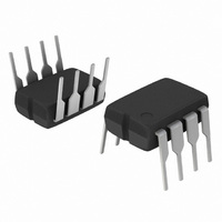
UC3842BNG ON Semiconductor, UC3842BNG Datasheet - Page 4

UC3842BNG
Manufacturer Part Number
UC3842BNG
Description
IC CTLR CURRENT MODE 8-DIP
Manufacturer
ON Semiconductor
Type
Pulse Width Modulator Controllerr
Specifications of UC3842BNG
Pwm Type
Current Mode
Number Of Outputs
1
Frequency - Max
275kHz
Duty Cycle
96%
Voltage - Supply
11.5 V ~ 25 V
Buck
No
Boost
Yes
Flyback
Yes
Inverting
No
Doubler
No
Divider
No
Cuk
No
Isolated
Yes
Operating Temperature
0°C ~ 70°C
Package / Case
8-DIP (0.300", 7.62mm)
Frequency-max
275kHz
Duty Cycle (max)
96 % (Typ)
Output Voltage
4.9 V to 5.1 V
Output Current
1000 mA (Max)
Mounting Style
Through Hole
Switching Frequency
500 KHz
Operating Supply Voltage
30 V
Maximum Operating Temperature
70 C
Fall Time
50 ns
Minimum Operating Temperature
0 C
Rise Time
50 ns
Synchronous Pin
No
Topology
Boost or Flyback or Forward
Current, Input Bias
-2 μA
Current, Output
+12 mA (Sink), -1 mA (Source)
Current, Supply
0.3 mA
Frequency, Oscillator
250 kHz
Package Type
PDIP-8
Power Dissipation
1.25 W
Regulation, Line
2 mV
Regulation, Load
3 mV
Regulator Type
DC-DC
Temperature, Operating, Range
0 to +70 °C
Time, Fall
50 ns
Time, Rise
50 ns
Voltage, Gain
3 V/V
Voltage, Input
2.5 V
Voltage, Noise
50 μV
Voltage, Output
5 V
Voltage, Output, High
6.2 V
Voltage, Output, Low
0.8 V
Voltage, Supply
30 V
Voltage, Supply, Rejection Ratio
70 dB
Lead Free Status / RoHS Status
Lead free / RoHS Compliant
Other names
UC3842BNGOS
Available stocks
Company
Part Number
Manufacturer
Quantity
Price
Part Number:
UC3842BNG
Manufacturer:
ON/安森美
Quantity:
20 000
7. Adjust V
8. Low duty cycle pulse techniques are used during test to maintain junction temperature as close to ambient as possible.
ELECTRICAL CHARACTERISTICS
T
OUTPUT SECTION
UNDERVOLTAGE LOCKOUT SECTION
PWM SECTION
TOTAL DEVICE
A
Output Voltage
High State
Output Voltage with UVLO Activated (V
Output Voltage Rise Time (C
Output Voltage Fall Time (C
Startup Threshold (V
Minimum Operating Voltage After Turn−On (V
Duty Cycle
Power Supply Current
Power Supply Zener Voltage (I
T
T
is the operating ambient temperature range that applies [Note 8], unless otherwise noted.)
Low State (I
low
high
Maximum UC284XB, UC384XB
Maximum
Minimum
Startup (V
Startup
(Note 7)
= 0°C for UC3842B, UC3843B; −25°C for UC2842B, UC2843B; −40°C for UC3842BV, UC3843BV
= +70°C for UC3842B, UC3843B; +85°C for UC2842B, UC2843B; +105°C for UC3842BV, UC3843BV
CC
V
above the Startup threshold before setting to 15 V.
(I
(I
(I
CC
CC
UC384XBV
Sink
Sink
Source
Source
14 V for UCX842B, BV)
= 6.5 V for UCX843B,
= 20 mA)
= 200 mA)
CC
= 20 mA)
= 200 mA)
Characteristics
)
L
L
= 1.0 nF, T
= 1.0 nF, T
CC
= 25 mA)
CC
J
UC284XB, UC384XB
UC384XBV
UC284XB, UC384XB
UC384XBV
= 6.0 V, I
(V
J
= 25°C)
= 25°C)
CC
CC
= 15 V [Note 7], R
)
Sink
UCX842B, BV
UCX843B, BV
UCX842B, BV
UCX843B, BV
= 1.0 mA)
http://onsemi.com
T
= 10 k, C
V
4
Symbol
V
DC
DC
I
OL(UVLO)
CC
CC(min)
V
V
V
V
(max)
OH
t
t
OL
(min)
th
+ I
r
f
Z
C
T
= 3.3 nF. For typical values T
Min
7.8
9.0
7.0
13
12
15
94
30
−
−
−
−
−
−
−
−
−
−
−
UC284XB
13.5
13.4
Typ
0.1
1.6
0.1
8.4
7.6
0.3
50
50
16
10
96
12
36
−
−
−
−
Max
150
150
0.4
2.2
1.1
9.0
8.2
0.5
17
11
17
−
−
−
−
−
−
0
−
A
12.9
14.5
Min
7.8
8.5
7.0
13
12
94
93
30
−
−
−
−
−
−
−
−
−
= 25°C, for min/max values
UC384XB, XBV
13.5
13.5
13.4
Typ
0.1
1.6
1.6
0.1
8.4
7.6
0.3
50
50
16
10
96
96
12
36
−
Max
17.5
11.5
150
150
0.4
2.2
2.3
1.1
9.0
8.2
0.5
17
−
−
−
−
−
0
−
Unit
mA
ns
ns
%
V
V
V
V
V


