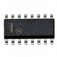
SG3525ADWG ON Semiconductor, SG3525ADWG Datasheet - Page 3

SG3525ADWG
Manufacturer Part Number
SG3525ADWG
Description
IC PWM SMPS CONTROLLER 16-SOIC
Manufacturer
ON Semiconductor
Datasheet
1.SG3525ADWR2G.pdf
(10 pages)
Specifications of SG3525ADWG
Pwm Type
Voltage Mode
Number Of Outputs
2
Frequency - Max
400kHz
Duty Cycle
49%
Voltage - Supply
8 V ~ 35 V
Buck
No
Boost
No
Flyback
No
Inverting
No
Doubler
No
Divider
No
Cuk
No
Isolated
No
Operating Temperature
0°C ~ 70°C
Package / Case
16-SOIC (0.300", 7.5mm Width)
Frequency-max
400kHz
Topology
Half-Bridge, Push-Pull
Output Current
400 mA
Switching Frequency
400 KHz
Duty Cycle (max)
49 %
Maximum Operating Temperature
+ 70 C
Minimum Operating Temperature
0 C
Fall Time
50 ns
Mounting Style
SMD/SMT
Rise Time
100 ns
Synchronous Pin
Yes
Lead Free Status / RoHS Status
Lead free / RoHS Compliant
Available stocks
Company
Part Number
Manufacturer
Quantity
Price
Maximum ratings are those values beyond which device damage can occur. Maximum ratings applied to the device are individual stress limit
values (not normal operating conditions) and are not valid simultaneously. If these limits are exceeded, device functional operation is not implied,
damage may occur and reliability may be affected.
1. Derate at 10 mW/ C for ambient temperatures above +50 C.
2. Derate at 16 mW/ C for case temperatures above +25 C.
Shutdown Options (See Block Diagram, page 2)
(Pins 9 and 8) have current source pull−ups, either can
readily accept a pull−down signal which only has to sink a
maximum of 100 mA to turn off the outputs. This is subject
to the added requirement of discharging whatever external
capacitance may be attached to these pins.
of Pin 10 which has been improved to enhance the available
shutdown options. Activating this circuit by applying a
positive signal on Pin 10 performs two functions: the PWM
MAXIMUM RATINGS
RECOMMENDED OPERATING CONDITIONS
Supply Voltage
Collector Supply Voltage
Logic Inputs
Analog Inputs
Output Current, Source or Sink
Reference Output Current
Oscillator Charging Current
Power Dissipation
Thermal Resistance, Junction−to−Air
Thermal Resistance, Junction−to−Case
Operating Junction Temperature
Storage Temperature Range
Lead Temperature (Soldering, 10 seconds)
Supply Voltage
Collector Supply Voltage
Output Sink/Source Current
Reference Load Current
Oscillator Frequency Range
Oscillator Timing Resistor
Oscillator Timing Capacitor
Deadtime Resistor Range
Operating Ambient Temperature Range
Since both the compensation and soft−start terminals
An alternate approach is the use of the shutdown circuitry
(Steady State)
(Peak)
T
T
A
C
= +25 C (Note 1)
= +25 C (Note 2)
Characteristics
Rating
APPLICATION INFORMATION
http://onsemi.com
SG3525A
3
latch is immediately set providing the fastest turn−off signal
to the outputs; and a 150 mA current sink begins to discharge
the external soft−start capacitor. If the shutdown command
is short, the PWM signal is terminated without significant
discharge of the soft−start capacitor, thus, allowing, for
example, a convenient implementation of pulse−by−pulse
current limiting. Holding Pin 10 high for a longer duration,
however, will ultimately discharge this external capacitor,
recycling slow turn−on upon release.
conceivably interrupt normal operation.
Pin 10 should not be left floating as noise pickup could
Symbol
Symbol
T
R
R
V
V
T
Solder
f
R
V
I
P
V
I
R
C
T
osc
T
I
I
qJC
ref
qJA
stg
ref
CC
CC
O
O
A
C
D
J
C
T
D
T
0.001
Min
8.0
4.5
0.1
2.0
0
0
0
0
0
−0.3 to +5.5
−55 to +125
−0.3 to V
Value
1000
2000
+150
+300
+40
+40
100
5.0
500
50
60
CC
Max
400
150
500
+70
0.2
35
35
100
400
20
Unit
Unit
Vdc
Vdc
mW
Vdc
Vdc
kHz
mA
mA
mA
C/W
C/W
mA
mA
kW
mF
V
V
W
C
C
C
C


