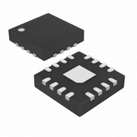
MAX8598ETE+T Maxim Integrated Products, MAX8598ETE+T Datasheet - Page 12

MAX8598ETE+T
Manufacturer Part Number
MAX8598ETE+T
Description
IC CNTRLR STP DWN LDO 16-TQFN
Manufacturer
Maxim Integrated Products
Datasheet
1.MAX8597ETP.pdf
(24 pages)
Specifications of MAX8598ETE+T
Pwm Type
Controller
Number Of Outputs
1
Frequency - Max
1.4MHz
Duty Cycle
99.5%
Voltage - Supply
4.5 V ~ 28 V
Buck
Yes
Boost
No
Flyback
No
Inverting
No
Doubler
No
Divider
No
Cuk
No
Isolated
No
Operating Temperature
-40°C ~ 85°C
Package / Case
16-TQFN Exposed Pad
Frequency-max
1.4MHz
Lead Free Status / RoHS Status
Lead free / RoHS Compliant
current ramps down through the low-side MOSFET body
diode; 20ns after DH goes low, the low-side MOSFET
turns on, resulting in a lower voltage drop to increase effi-
ciency. The low-side MOSFET turns off at the rising edge
of the next clock pulse, and when its gate voltage dis-
charges to zero, the high-side MOSFET turns on and
another cycle starts.
These controllers also sense peak inductor current and
provide hiccup-overload and short-circuit protection
(see the Current Limit section). The MAX8597/
MAX8598/MAX8599 operate in forced-PWM mode
where the inductor current is always continuous. The
controller maintains constant switching frequency
under all loads, except under dropout conditions where
it skips DL pulses.
The MAX8597/MAX8598/MAX8599 DC-DC step-down
controllers sense the peak inductor current either with
the on-resistance of the high-side MOSFET for lossless
sensing, or a series resistor for more accurate sensing.
When the voltage across the sensing element exceeds
the current-limit threshold set with ILIM, the controller
immediately turns off the high-side MOSFET. The low-
side MOSFET is then turned on to let the inductor cur-
rent ramp down. As the output load current increases
above the ILIM threshold, the output voltage sags
because the truncated duty cycle is insufficient to sup-
port the load current. When FB falls 30% below its nomi-
nal threshold, the output undervoltage protection is
triggered and the controller enters hiccup mode to limit
power dissipation. This current-limit method allows the
circuit to withstand a continuous output short circuit.
The MAX8597/MAX8598/MAX8599 current-limit thresh-
old is set by an external resistor that works in conjunc-
tion with an internal 200µA current sink (see the Setting
the Current Limit section for more details).
Synchronous rectification reduces the conduction loss
in the rectifier by replacing the normal Schottky catch
diode with a low-resistance MOSFET switch. The
MAX8597/MAX8598/MAX8599 also use the synchro-
nous rectifier to ensure proper startup of the boost
gate-drive circuit.
Low-Dropout, Wide-Input-Voltage,
Step-Down Controllers
12
______________________________________________________________________________________
Synchronous-Rectifier Driver (DL)
Current Limit
Gate-drive voltage for the high-side n-channel MOSFET is
generated by an external flying capacitor and diode boost
circuit (D1 and C5 in Figure 1). When the synchronous
rectifier is on, C5 is charged from the VL supply through
the Schottky diode. When the synchronous rectifier is
turned off, the Schottky is reverse biased and the voltage
on C5 is stacked above LX to provide the necessary turn-
on voltage for the high-side MOSFET. A low-current
Schottky diode, such as Central Semiconductor’s
CMDSH-3, works well for most applications. The capacitor
should be large enough to prevent it from charging to
excessive voltage, but small enough to adequately charge
during the minimum low-side MOSFET on-time, which
occurs at minimum input voltage. A capacitor in the 0.1µF
to 0.47µF range works well for most applications.
The MAX8597/MAX8598/MAX8599 contain a low-
dropout 5V regulator that provides up to 35mA to sup-
ply gate drive for the external MOSFETs, and supplies
AVL, which powers the IC’s internal circuitry. Bypass
the regulator’s output (VL) with 1µF per 10mA of VL
load, or greater ceramic capacitor. The current
required to drive the external MOSFET can be estimat-
ed by multiplying the total gate charge (at V
the MOSFETs by the switching frequency.
When V
MAX8598/MAX8599s’ undervoltage-lockout (UVLO) cir-
cuitry inhibits switching, forces POK (MAX8598/
MAX8599) low, and forces DH and DL low. Once V
rises above 4.2V (typ), the controller powers up the out-
put in startup mode (see the Startup section).
The MAX8597/MAX8598/MAX8599 start switching once
all the following conditions are met:
1) EN is high.
2) V
3) Soft-start voltage V
4) Thermal limit is not exceeded.
The third condition ensures that the MAX8597/
MAX8598/MAX8599 do not discharge a prebiased out-
put. Once all of these conditions are met, the IC begins
switching and the soft-start cycle is initiated.
VL
> 4.2V (typ).
VL
High-Side Gate-Drive Supply (BST)
drops below 3.75V (typ), the MAX8597/
Undervoltage Lockout (UVLO)
Internal 5V Linear Regulator
SS
exceeds V
FB
.
GS
Startup
= 5V) of
VL


