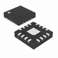
MAX8599ETE+T Maxim Integrated Products, MAX8599ETE+T Datasheet - Page 11

MAX8599ETE+T
Manufacturer Part Number
MAX8599ETE+T
Description
IC CNTRLR STP DWN LDO 16-TQFN
Manufacturer
Maxim Integrated Products
Datasheet
1.MAX8597ETP.pdf
(24 pages)
Specifications of MAX8599ETE+T
Pwm Type
Controller
Number Of Outputs
1
Frequency - Max
1.4MHz
Duty Cycle
99.5%
Voltage - Supply
4.5 V ~ 28 V
Buck
Yes
Boost
No
Flyback
No
Inverting
No
Doubler
No
Divider
No
Cuk
No
Isolated
No
Operating Temperature
-40°C ~ 85°C
Package / Case
16-TQFN Exposed Pad
Frequency-max
1.4MHz
Lead Free Status / RoHS Status
Lead free / RoHS Compliant
The MAX8597/MAX8598/MAX8599 voltage-mode PWM
step-down controllers are designed to operate from
4.5V to 28V input and generate output voltages down to
0.6V. A proprietary switching algorithm stretches the
duty cycle to >99.5% for low-dropout design. Unlike
conventional step-down regulators using a p-channel
high-side MOSFET to achieve high duty cycle, the
MAX8597/MAX8598/MAX8599 drive n-channel
MOSFETs permitting high efficiency and high-current
designs.
The MAX8597 is available in a 20-pin thin QFN pack-
age and is designed for applications that use an ana-
log signal to control the output voltage with adjustable
offset, such as DC fan speed control. For example, a
12VDC fan can be driven from 6V to 12V with 12V input
power source depending on the system’s cooling
requirement to minimize fan noise and power consump-
tion. This is achieved with an internal uncommitted
operational amplifier. With the addition of an external
RC filter, a PWM input can also be used to control the
output voltage. The MAX8597 also generates a tracking
output for chipsets, ASICs, and DSP where core and
I/O supplies are split and require tracking. In applica-
tions where tighter output tolerance is required, the
MAX8597 output can be set by an external precision
reference source feeding to REFIN. The MAX8598/
MAX8599 are available in a 16-pin thin QFN package
and do not have the uncommitted operational amplifier,
reference input, and reference output, but offer a power-
OK output (POK). With the enable input and POK out-
put, the MAX8598/MAX8599 can easily be configured to
have power sequencing of multiple supply rails.
MAX8597
17
18
19
20
—
—
PIN
MAX8598/
MAX8599
15
16
—
—
—
—
______________________________________________________________________________________
Detailed Description
NAME
AOUT
FREQ
AIN+
AIN-
POK
EP
Frequency Adjust Input. Connect a resistor from FREQ to GND to set the switching frequency.
The range of the FREQ resistor is 14.3kΩ to 100kΩ (corresponding to 1400kHz to 200kHz).
Output of the Uncommitted Operational Amplifier. AOUT is high impedance during
undervoltage lockout.
Inverting Input of the Uncommitted Operational Amplifier
Noninverting Input of the Uncommitted Operational Amplifier
Power-OK Output. POK is an open-drain output that goes high impedance when the regulator
output is greater than 88% of the regulation threshold. POK is low during shutdown.
Exposed Paddle. Connect to analog ground plane for improved thermal performance.
Low-Dropout, Wide-Input-Voltage,
The MAX8597/MAX8598/MAX8599 allow startup with
prebias voltage on the output for applications where a
backup supply or a tracking device may charge the
output capacitor before the MAX8597/MAX8598/
MAX8599 are enabled. The MAX8599 has output over-
voltage protection.
These controllers feature lossless high-side peak
inductor current sensing, adjustable current limit, and
hiccup-mode short-circuit protection. Switching fre-
quency is set with an external resistor from 200kHz to
1.4MHz. This wide frequency range combined with a
wide-bandwidth error amplifier enable the loop-com-
pensation scheme to give the user ample flexibility to
optimize for cost, size, and efficiency.
The MAX8597/MAX8598/MAX8599 step-down DC-DC
controllers use a PWM voltage-mode control scheme. An
internal high-bandwidth (25MHz) operational amplifier is
used as an error amplifier to regulate the output voltage.
The output voltage is sensed and compared with an inter-
nal 0.6V reference or REFIN (MAX8597) to generate an
error signal. The error signal is then compared with a
fixed-frequency ramp by a PWM comparator to give the
appropriate duty cycle to maintain output voltage regula-
tion. The high-side MOSFET turns on at the rising edge of
the internal clock 20ns after DL (the low-side MOSFET
gate drive) goes low. The high-side MOSFET turns off
once the internal ramp voltage reaches the error-amplifier
output voltage. The process repeats for every clock
cycle. During the high-side MOSFET on-time, current
flows from the input through the inductor to the output
capacitor and load. At the moment the high-side MOS-
FET turns off, the energy stored in the inductor during the
on-time is released to support the load as the inductor
Step-Down Controllers
FUNCTION
Pin Description (continued)
DC-DC Controller
11


