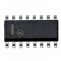
MC33023DWR2G ON Semiconductor, MC33023DWR2G Datasheet - Page 3

MC33023DWR2G
Manufacturer Part Number
MC33023DWR2G
Description
IC CTRLR PWM HS SGL ENDED 16SOIC
Manufacturer
ON Semiconductor
Datasheet
1.MC33023DWR2G.pdf
(18 pages)
Specifications of MC33023DWR2G
Pwm Type
Voltage/Current Mode
Number Of Outputs
1
Frequency - Max
1MHz
Duty Cycle
90%
Voltage - Supply
10 V ~ 30 V
Buck
No
Boost
No
Flyback
No
Inverting
No
Doubler
No
Divider
No
Cuk
No
Isolated
Yes
Operating Temperature
-40°C ~ 105°C
Package / Case
16-SOIC (0.300", 7.5mm Width)
Frequency-max
1MHz
Duty Cycle (max)
90 %
Output Voltage
5.05 V to 5.15 V
Output Current
500 mA
Mounting Style
SMD/SMT
Switching Frequency
1000 KHz
Operating Supply Voltage
30 V
Maximum Operating Temperature
+ 105 C
Fall Time
30 ns
Minimum Operating Temperature
- 40 C
Rise Time
30 ns
Synchronous Pin
Yes
Topology
Flyback, Forward
Number Of Pwm Outputs
1
On/off Pin
Yes
Adjustable Output
No
Switching Freq
1MHz
Operating Supply Voltage (max)
30V
Operating Temperature Classification
Industrial
Mounting
Surface Mount
Pin Count
16
Package Type
SOIC W
Lead Free Status / RoHS Status
Lead free / RoHS Compliant
Other names
MC33023DWR2GOS
Available stocks
Company
Part Number
Manufacturer
Quantity
Price
1. Maximum package power dissipation limits must be observed.
2. Low duty cycle pulse techniques are used during test to maintain junction temperature as close to ambient as possible.
ELECTRICAL CHARACTERISTICS
is the operating ambient temperature range that applies [Note 2], unless otherwise noted.)
REFERENCE SECTION
OSCILLATOR SECTION
ERROR AMPLIFIER SECTION
PWM COMPARATOR SECTION
SOFT−START SECTION
Reference Output Voltage (I
Line Regulation (V
Load Regulation (I
Temperature Stability
Total Output Variation over Line, Load, and Temperature
Output Noise Voltage (f = 10 Hz to 10 kHz, T
Long Term Stability (T
Output Short Circuit Current
Frequency
Frequency Change with Voltage (V
Frequency Change with Temperature (T
Sawtooth Peak Voltage
Sawtooth Valley Voltage
Clock Output Voltage
Input Offset Voltage
Input Bias Current
Input Offset Current
Open−Loop Voltage Gain (V
Gain Bandwidth Product (T
Common Mode Rejection Ratio (V
Power Supply Rejection Ratio (V
Output Current, Source (V
Output Current,
Output Voltage Swing, High State (I
Output Voltage Swing,
Slew Rate
Ramp Input Bias Current
Duty Cycle, Maximum
Duty Cycle,
Zero Duty Cycle Threshold Voltage Pin 3(4) (Pin 7(9) = 0 V)
Propagation Delay (Ramp Input to Output, T
Charge Current (V
Discharge Current (V
T
T
Line (V
High State
Low State
low
J
= + 25°C
= 0°C for MC34023
= −40°C for MC33023
CC
= 10 V to 30 V) and Temperature (T
Minimum
Sink (V
O
Soft−Start
CC
= 1.0 mA to 10 mA)
Soft−Start
A
= 10 V to 30 V)
= +125°C for 1000 Hours)
Low State (I
O
= 1.0 V)
O
J
= 0.5 V)
O
O
= + 25°C)
= 4.0 V)
= 1.0 mA, T
= 1.5 V)
= 1.0 V to 4.0 V)
Characteristic
CC
CM
CC
O
= 10 V to 30 V)
O
= 1.5 V to 5.5 V)
= 1 mA)
= 10 V to 30 V)
= − 0.5 mA)
A
(V
= T
J
= + 25°C)
CC
J
J
low
= + 25°C)
= + 25°C)
= 15 V, R
A
to T
T
= T
high
high
low
= +70°C for MC34023
= +105°C for MC33023
)
T
http://onsemi.com
to T
= 3.65 kW, C
high
)
3
T
= 1.0 nF, for typical values T
t
Df
Df
PLH(in/out)
Symbol
V
V
DC
Reg
DC
Reg
CMRR
I
PSRR
I
GBW
Source
OSC(P)
OSC(V)
A
dischg
osc
osc
V
I
V
V
V
V
V
f
I
I
V
SR
Sink
V
T
V
I
osc
I
VOL
I
chg
SC
S
(max)
OH
IB
IO
OH
IB
OL
OL
(min)
ref
ref
IO
S
th
n
load
line
/DV
/DT
5.05
4.95
− 30
Min
380
370
2.6
0.7
3.9
4.0
0.5
1.0
4.5
6.0
1.1
3.0
1.0
60
75
85
80
−
−
−
−
−
−
−
−
−
−
−
0
−
−
−
A
= + 25°C, for min/max values T
− 65
4.75
−0.5
1.25
Typ
400
400
110
5.1
2.0
2.0
0.2
5.0
0.2
2.0
2.8
1.0
4.5
2.3
0.6
0.1
8.3
3.0
3.6
0.4
9.0
4.0
50
95
95
12
90
60
−
−
−
−100
−5.0
Max
5.15
5.25
1.25
420
430
100
1.0
3.0
2.9
3.0
1.0
5.0
1.0
1.4
15
15
15
20
−
−
−
−
−
−
−
−
−
−
−
−
−
0
−
mV/°C
MHz
Unit
V/ms
kHz
mV
mV
mV
mA
mV
mA
mA
mV
mA
mA
dB
dB
dB
mA
mA
ns
%
%
%
V
V
V
V
V
V
V
A


