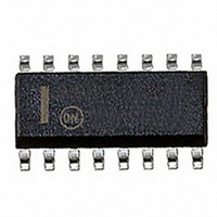
MC34025DWG ON Semiconductor, MC34025DWG Datasheet - Page 10

MC34025DWG
Manufacturer Part Number
MC34025DWG
Description
IC CTRLR PWM DBL END HF 16SOIC
Manufacturer
ON Semiconductor
Datasheet
1.MC34025DWR2G.pdf
(20 pages)
Specifications of MC34025DWG
Pwm Type
Voltage/Current Mode
Number Of Outputs
2
Frequency - Max
1MHz
Duty Cycle
45%
Voltage - Supply
10 V ~ 30 V
Buck
No
Boost
No
Flyback
No
Inverting
No
Doubler
No
Divider
No
Cuk
No
Isolated
Yes
Operating Temperature
0°C ~ 70°C
Package / Case
16-SOIC (0.300", 7.5mm Width)
Frequency-max
1MHz
Duty Cycle (max)
45 %
Output Voltage
5.05 V to 5.15 V
Output Current
500 mA
Mounting Style
SMD/SMT
Switching Frequency
1000 KHz
Operating Supply Voltage
30 V
Maximum Operating Temperature
+ 70 C
Fall Time
30 ns
Minimum Operating Temperature
0 C
Rise Time
30 ns
Synchronous Pin
Yes
Topology
Half-Bridge, Push-Pull
Lead Free Status / RoHS Status
Lead free / RoHS Compliant
Other names
MC34025DWGOS
Available stocks
Company
Part Number
Manufacturer
Quantity
Price
Part Number:
MC34025DWG
Manufacturer:
ON/安森美
Quantity:
20 000
DIP/SOIC
In voltage mode operation, the control range on the output of
the Error Amplifier from 0% to 90% duty cycle is from 2.25 V
to 4.05 V.
Pin No.
10
12
13
14
15
16
11
1
2
3
4
5
6
7
8
9
Feedback Input
Output Voltage
Figure 22. Voltage Mode Operation
Error Amp Inverting
Input
Error Amp
Noninverting Input
Error Amp Output
Clock
R
C
Ramp Input
Soft−Start
Current
Limit/Shutdown
Ground
Output A
Power Ground
V
Output B
V
V
C
C
CC
ref
T
T
T
Function
V
ref
4
5
6
7
3
1
2
This pin is usually used for feedback from the output of the power supply.
This pin is used to provide a reference in which an error signal can be produced on the output of the
error amp. Usually this is connected to V
This pin is provided for compensating the error amp for poles and zeros encountered in the power
supply system, mostly the output LC filter.
This is a bidirectional pin used for synchronization.
The value of R
In conjunction with R
push−pull output, each output runs at one−half the frequency set at this pin.
For voltage mode operation this pin is connected to C
connected through a filter to the current sensing element.
A capacitor at this pin sets the Soft−Start time.
This pin has two functions. First, it provides cycle−by−cycle current limiting. Second, if the current is
excessive, this pin will reinitiate a Soft−Start cycle.
This pin is the ground for the control circuitry.
This is a high current totem pole output.
This is a separate power ground return that is connected back to the power source. It is used to
reduce the effects of switching transient noise on the control circuitry.
This is a separate power source connection for the outputs that is connected back to the power
source input. With a separate power source connection, it can reduce the effects of switching
transient noise on the control circuitry.
This is a high current totem pole output.
This pin is the positive supply of the control IC.
This is a 5.1 V reference. It is usually connected to the noninverting input of the error amplifier.
1.25 V
Oscillator
PIN FUNCTION DESCRIPTION
T
sets the charge current through timing Capacitor, C
T
http://onsemi.com
, the timing Capacitor sets the switching frequency. Because this part is a
10
In current mode control, an RC filter should be placed at the
ramp input to filter the leading edge spike caused by turn−on of
a power MOSFET.
Sense Element
From Current
ref
, however an external reference can also be used.
Feedback Input
Output Voltage
Description
Figure 23. Current Mode Operation
T
. For current mode operation this pin is
C
T
V
ref
4
5
6
7
3
1
2
T
.
1.25 V
Oscillator


