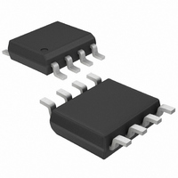
MAX5019CSA+ Maxim Integrated Products, MAX5019CSA+ Datasheet - Page 10

MAX5019CSA+
Manufacturer Part Number
MAX5019CSA+
Description
IC CNTRLR PWM CRNT MD 8-SOIC
Manufacturer
Maxim Integrated Products
Datasheet
1.MAX5020ESA.pdf
(14 pages)
Specifications of MAX5019CSA+
Pwm Type
Current Mode
Number Of Outputs
1
Frequency - Max
302kHz
Duty Cycle
85%
Voltage - Supply
13 V ~ 110 V
Buck
No
Boost
No
Flyback
Yes
Inverting
No
Doubler
No
Divider
No
Cuk
No
Isolated
Yes
Operating Temperature
0°C ~ 70°C
Package / Case
8-SOIC (3.9mm Width)
Frequency-max
302kHz
Duty Cycle (max)
85 %
Output Current
1000 mA
Mounting Style
SMD/SMT
Switching Frequency
275 KHz
Maximum Operating Temperature
+ 70 C
Minimum Operating Temperature
0 C
Synchronous Pin
No
Topology
Flyback, Forward
Lead Free Status / RoHS Status
Lead free / RoHS Compliant
pass filter (Figures 2, 3). Select the current-sense resis-
tor, R
where I
current.
When V
The propagation delay from the time the switch current
reaches the trip level to the driver turn-off time is 180ns.
The MAX5019/MAX5020 include an internal error ampli-
fier that can be used to regulate the output voltage in
the case of a nonisolated power supply (see Figure 2).
Calculate the output voltage using the following equa-
tion:
where V
Choose R
resistance of FB. The gain of the error amplifier is inter-
nally configured for -20 (see Figure 1).
The error amplifier may also be used to regulate the out-
put of the tertiary winding for implementing a primary-
side regulated isolated power supply (see Figure 4).
Calculate the output voltage using the following equation:
where N
the number of tertiary winding turns.
An internal 275kHz oscillator determines the switching
frequency of the controller. At the beginning of each
cycle, NDRV switches the N-channel MOSFET on.
NDRV switches the external MOSFET off after the maxi-
mum duty cycle has been reached, regardless of the
feedback.
The MAX5019 uses an internal ramp generator for
slope compensation. The internal ramp signal is reset
at the beginning of each cycle and slews at 26mV/µs.
The PWM comparator uses the instantaneous current,
the error voltage, the internal reference, and the slope
compensation (MAX5019 only) to determine when to
Current-Mode PWM Controllers with Integrated
Startup Circuit
10
PWM Comparator and Slope Compensation
______________________________________________________________________________________
SENSE
LimPrimary
CS
REF
S
1
is the number of secondary turns and N
//R
> 465mV, the power MOSFET switches off.
according to the following equation:
= 2.4V.
R
2
SENSE
V
V
<< R
OUT
OUT
is the maximum peak primary-side
=
= 0 465
=
IN
N
N
, where R
.
S
T
1
+
Internal Error Amplifier
1
R
R
/ V
+
1
2
R
×
R
I
LimPrimary
1
2
×
IN
V
REF
, ≅ 50kΩ is the input
V
REF
T
is
switch the N-channel MOSFET off. In normal operation
the N-channel MOSFET turns off when:
where I
MOSFET, V
output voltage of the internal amplifier, and V
a ramp function starting at 0 and slewing at 26mV/µs
(MAX5019 only). When using the MAX5019 in a for-
ward-converter configuration the following condition
must be met to avoid control-loop subharmonic oscilla-
tions:
where k = 0.75 to 1, and N
turns on the secondary and primary side of the trans-
former, respectively. L is the output filter inductor. This
makes the output inductor current downslope as refer-
enced across R
tion. The controller responds to transients within one
cycle when this condition is met.
NDRV drives an N-channel MOSFET. NDRV sources
and sinks large transient currents to charge and dis-
charge the MOSFET gate. To support such switching
transients, bypass V
average current as a result of switching the MOSFET is
the product of the total gate charge and the operating
frequency. It is this current plus the DC quiescent cur-
rent that determines the total operating current.
The following is a general procedure for designing a
forward converter using the MAX5020.
The circuit in Figure 2 was designed as follows:
1) Determine the requirements.
2) Set the output voltage.
3) Calculate the transformer primary to secondary
4) Calculate the reset to primary winding turns ratio.
5) Calculate the tertiary to primary winding turns
6) Calculate the current-sense resistor value.
7) Calculate the output inductor value.
8) Select the output capacitor.
winding turns ratio.
ratio.
PRIMARY
I
PRIMARY
REF
N
N
S
P
N-Channel MOSFET Gate Driver
is the 2.4V internal reference, V
Applications Information
×
SENSE
is the current through the N-channel
×
k R
×
R
SENSE
CC
SENSE
equal to the slope compensa-
with a ceramic capacitor. The
L
S
>
×
and N
V
V
EA
OUT
- V
Design Example
=
P
REF
26
are the number of
mV
- V
/
SCOMP
µ
s
SCOMP
EA
is the
is


