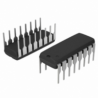
TL494CN ON Semiconductor, TL494CN Datasheet - Page 2

TL494CN
Manufacturer Part Number
TL494CN
Description
IC PWM VM 16DIP
Manufacturer
ON Semiconductor
Series
SWITCHMODE™r
Datasheet
1.TL494CDR2G.pdf
(14 pages)
Specifications of TL494CN
Pwm Type
Voltage Mode
Number Of Outputs
1
Frequency - Max
200kHz
Duty Cycle
50%
Voltage - Supply
7 V ~ 40 V
Buck
No
Boost
No
Flyback
No
Inverting
No
Doubler
No
Divider
No
Cuk
No
Isolated
No
Operating Temperature
0°C ~ 70°C
Package / Case
16-DIP (0.300", 7.62mm)
Frequency-max
200kHz
Topology
Boost, Buck, Flyback, Forward, Full-Bridge, Half-Bridge, Push-Pull
Output Voltage
40 V
Output Current
200 mA
Switching Frequency
300 KHz
Duty Cycle (max)
45 %
Operating Supply Voltage
15 V
Maximum Operating Temperature
+ 70 C
Minimum Operating Temperature
0 C
Fall Time
40 ns
Mounting Style
Through Hole
Rise Time
100 ns
Synchronous Pin
No
Lead Free Status / RoHS Status
Contains lead / RoHS non-compliant
Other names
TL494CNOS
Available stocks
Company
Part Number
Manufacturer
Quantity
Price
Part Number:
TL494CN
Manufacturer:
TI/德州仪器
Quantity:
20 000
Company:
Part Number:
TL494CN/UPC494C
Manufacturer:
TI/NEC/KIA
Quantity:
5 510
Part Number:
TL494CNG
Manufacturer:
TI/德州仪器
Quantity:
20 000
Part Number:
TL494CNSR
Manufacturer:
TI/德州仪器
Quantity:
20 000
RECOMMENDED OPERATING CONDITIONS
ELECTRICAL CHARACTERISTICS
For typical values T
REFERENCE SECTION
OUTPUT SECTION
2. Low duty cycle pulse techniques are used during test to maintain junction temperature as close to ambient temperature as possible.
Power Supply Voltage
Collector Output Voltage
Collector Output Current (Each transistor)
Amplified Input Voltage
Current Into Feedback Terminal
Reference Output Current
Timing Resistor
Timing Capacitor
Oscillator Frequency
Reference Voltage (I
Line Regulation (V
Load Regulation (I
Short Circuit Output Current (V
Collector Off−State Current
Emitter Off−State Current
Collector−Emitter Saturation Voltage (Note 2)
Output Control Pin Current
Output Voltage Rise Time
Output Voltage Fall Time
(V
V
Common−Emitter (V
Emitter−Follower (V
Low State (V
High State (V
Common−Emitter (See Figure 12)
Emitter−Follower (See Figure 13)
Common−Emitter (See Figure 12)
Emitter−Follower (See Figure 13)
CC
CC
= 40 V, V
= 40 V, V
OC
OC
C
CE
A
= 40 V, V
O
CC
v 0.4 V)
= V
= 25°C, for min/max values T
= 40 V)
= 1.0 mA to 10 mA)
O
= 7.0 V to 40 V)
C
ref
= 1.0 mA)
E
= 15 V, I
= 0 V, I
)
Characteristics
Characteristics
E
= 0 V)
ref
C
E
= 200 mA)
= 0 V)
= −200 mA)
(V
CC
= 15 V, C
A
is the operating ambient temperature range that applies, unless otherwise noted.
T
TL494, NCV494
http://onsemi.com
= 0.01 mF, R
2
T
= 12 kW, unless otherwise noted.)
V
Symbol
Symbol
Reg
I
Reg
V
V
C1
C1
I
I
I
I
V
C(off)
V
E(off)
f
sat(C)
sat(E)
OCH
V
I
OCL
l
R
C
osc
l
SC
ref
, V
, I
t
CC
fb
t
ref
in
r
f
T
T
load
line
C2
C2
0.0047
−0.3
4.75
Min
Min
7.0
1.8
1.0
15
−
−
−
−
−
−
−
−
−
−
−
−
−
−
−
−
0.001
Typ
Typ
100
100
5.0
2.0
3.0
2.0
1.1
1.5
0.2
15
30
30
40
35
10
25
40
−
−
−
−
−
V
CC
−100
Max
Max
5.25
200
500
200
100
200
200
100
100
0.3
1.3
2.5
3.5
40
40
10
10
25
15
75
−
− 2.0
Unit
Unit
kHz
mA
mA
mA
mV
mV
mA
mA
kW
mF
mA
mA
mA
ns
ns
V
V
V
V
V


