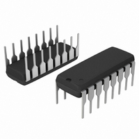
MC44604P ON Semiconductor, MC44604P Datasheet - Page 17

MC44604P
Manufacturer Part Number
MC44604P
Description
IC CTRLR PWM FREQ PULSED 16DIP
Manufacturer
ON Semiconductor
Series
GreenLine™r
Type
High Performance Pulsed Mode PWM Contollerr
Datasheet
1.MC44604P.pdf
(22 pages)
Specifications of MC44604P
Pwm Type
Current Mode
Number Of Outputs
1
Frequency - Max
250kHz
Duty Cycle
82%
Voltage - Supply
10 V ~ 15 V
Buck
No
Boost
No
Flyback
Yes
Inverting
No
Doubler
No
Divider
No
Cuk
No
Isolated
No
Operating Temperature
-25°C ~ 85°C
Package / Case
16-DIP (0.300", 7.62mm)
Frequency-max
250kHz
Input Voltage Range
18 V
Mounting Style
Through Hole
Lead Free Status / RoHS Status
Contains lead / RoHS non-compliant
Other names
MC44604POS
Available stocks
Company
Part Number
Manufacturer
Quantity
Price
Company:
Part Number:
MC44604P
Manufacturer:
ON
Quantity:
1 765
Part Number:
MC44604P
Manufacturer:
ON/安森美
Quantity:
20 000
Company:
Part Number:
MC44604P2
Manufacturer:
IR
Quantity:
6 882
connected to pin 11), an internal zener diode (D
Figure 34) is able to clamp the pin 11 voltage to a value V
that is higher than the oscillator value and so, that results in
no max duty cycle limitation.
generated until the V
(refer to the undervoltage lockout section paragraph).
During the delay between the disable 1 and the disable 2,
using a transistor controlled by UVLO1, the pin 11 voltage
is made equal to zero in order to make the max duty cycle and
soft−start arrangement ready to work for the next restart.
interfere with the Standby Current Set.
Protection
thanks to the protection it offers.
Demagnetization Detection (Refer to Demag §)
Foldback
enables to reduce the maximum V
equal to 1 typically, if there was no foldback action. Finally,
the foldback arrangement is a programmable peak current
limitation.
gradually increasing voltage) but in fact, it has been
designed to provide the system with an effective overload
protection.
required converter peak current becomes higher and so,
Pin 11
In any case (particularly if no external component is
As soon as V
In standby mode, this block is inhibited in order not to
The MC44604 can ensure a high converter reliability
As depicted in Figure 28, the foldback input (pin 5)
It could be used as a soft−start (by connecting to pin 5, a
Indeed, as the output load gradually increases, the
RI
V
Nominal
disable2
Figure 35. Different Possible Uses of Pin 11
V
V
CC
V
O
R Connected to
out
Figure 36. Foldback Characteristic
I = 0.4 I
Pin 11
disable1
ref
V
CC
Z
Sequence Initiated
is detected, a signal UVLO1 is
voltage falls down to V
New Startup
C
CS
value that would be
I
pk max
V
RI
Z
Overload
C // R
Z
, refer to
τ = RC
I
out
disable2
http://onsemi.com
Z
17
V
V
not able to supply enough energy to maintain the output
regulation. Consequently, the decreasing output can be used
to apply a voltage that diminishes to a value lower than 1 V,
to pin 5, in order to limit the maximum peak current. In this
way, the well known foldback characteristic is obtained
(refer to Figure 36).
5 to V
Overvoltage Protection
that compares the pin 6 voltage to V
Figure 37).
comparator non inverting input voltage is nearly equal to:
into account the overvoltages that last at least 2 ms.
output becomes high and as this level is brought back to the
input through an OR gate, V
the IC output is disabled) until V
detected, the output is disabled until a new circuit restart.
started−up in order to limit the circuit startup consumption
(T is switched on when once V
V
Pin 6
CS
CS max
Then if the output load keeps on increasing, the system is
The foldback action can be inhibited by connecting the pin
The overvoltage arrangement consists of a comparator
If no external component is connected to pin 6, the
So, the comparator output is high when:
A delay latch (2 ms) is incorporated in order to only take
If this condition is achieved, V
Consequently when an overvoltage longer than 2 ms is
The V
OVP
grows up till it reaches its maximum value (normally,
CC
V
.
= 1 V).
0
CC
CC
Figure 37. Overvoltage Protection
11.6 K
T
11, 6 kΩ ) 2 kΩ
2 K
is connected when once the circuit has
2.5 V
11, 6 kΩ ) 2 kΩ
2 kΩ
Enable
2.5 V
(V
ref
V
Delay
CC
2 kΩ
)
V
Out
In
ref
C
w 17 V
τ
OVLO
OVPout
•
ref
5.0 ms
V
CC
ref
has been generated).
OVPout
the Output is Disabled)
•
is disabled.
remains high (and so,
V
w 2, 5 V
CC
ref
(If V
In
Delay
2.0 ms
τ
(2,5 V) (refer to
OVP out
the delay latch
Out
= 1.0,
V
OVP out


