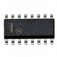
CS51221EDR16 ON Semiconductor, CS51221EDR16 Datasheet - Page 11

CS51221EDR16
Manufacturer Part Number
CS51221EDR16
Description
IC CTRLR PWM FFVOLT MODE 16SOIC
Manufacturer
ON Semiconductor
Datasheet
1.CS51221EDR16G.pdf
(14 pages)
Specifications of CS51221EDR16
Pwm Type
Voltage Mode
Number Of Outputs
1
Frequency - Max
1MHz
Duty Cycle
90%
Voltage - Supply
4.7 V ~ 15 V
Buck
Yes
Boost
No
Flyback
No
Inverting
No
Doubler
No
Divider
Yes
Cuk
No
Isolated
Yes
Operating Temperature
-40°C ~ 85°C
Package / Case
16-SOIC (3.9mm Width)
Frequency-max
1MHz
Topology
Buck, Flyback, Forward
Output Voltage
- 0.3 V to + 15 V
Output Current
1000 mA
Switching Frequency
1000 KHz
Duty Cycle (max)
90 %
Fall Time
25 ns
Mounting Style
SMD/SMT
Rise Time
60 ns
Synchronous Pin
Yes
Lead Free Status / RoHS Status
Contains lead / RoHS non-compliant
Other names
CS51221EDR16OSTR
Available stocks
Company
Part Number
Manufacturer
Quantity
Price
Company:
Part Number:
CS51221EDR16G
Manufacturer:
EPSON
Quantity:
890
Part Number:
CS51221EDR16G
Manufacturer:
ON/安森美
Quantity:
20 000
that during steady state, V
voltage variations. This intuitively explains why FF voltage
mode control has superior line regulation and line transient
response. Knowing the nominal value of V
can also select the value of RC to place V
of its dynamic range.
Select Feedback Voltage Divider
the FB pin, which connects to the inverting input of the error
amplifier. The non−inverting input of the error amplifier is
connected to a 1.27 V (typ) reference voltage. The FB pin
has an input current which has to be considered for accurate
DC outputs. The following equation can be used to calculate
the R1 and R2 value
where ∇ is the correction factor due to the existence of the
FB pin input current Ier.
divider output.
Design Voltage Dividers for OV and UV Detection
series to set OV and UV threshold seen from the input
voltage. The values of the resistors can be calculated from
the following three equations, where the third equation is
derived from OV hysteresis requirement.
As shown in Figure 12, the voltage divider output feeds to
Ri = DC resistance between the FB pin and the voltage
Ier = V
In Figure 13, the voltage divider uses three resistors in
800
700
600
500
400
300
200
100
0.0001
0
Figure 10. Typical Performance Characteristics,
V IN(HIGH)
V IN(LOW)
FB
input current, 1.3 mA typical.
R
R
T
T
R1 ) R2
= 10 K
= 50 K
Oscillator Frequency vs. C
R2
+ (Ri ) R1 R2)Ier
R2 ) R3 ) R1
R2 ) R3 ) R1
R
V OUT + 1.27 *
T
COMP
R2 ) R3
= 5.0 K
C
R3
0.001
T
(mF)
doesn’t change for input
COMP
+ 1.0 V
+ 2.0 V
IN
and T
T
at the center
ON
http://onsemi.com
, one
(A)
(B)
CS51221
0.01
11
1.00
0.95
0.90
0.85
0.80
0.75
0.70
0.65
0.60
0.55
0.50
where:
threshold;
design, V
V
to program OV and UV separately.
1000
IN(LOW)
V
V
It is self−evident from equation A and B that to use this
Figure 12. The Design of Feedback Voltage Divider
Has to Consider the Error Amplifier Input Current
IN(LOW)
HYST
Figure 11. Typical Performance Characteristics,
COMP
. Otherwise, two voltage dividers have to be used
V
= OV hysteresis seen at V
IN(HIGH)
IN
, V
Figure 13. OV/UV Monitor Divider
12.5 mA
Oscillator Duty Cycle vs. R
IN(HIGH)
10000
has to be two times greater than
R1
(R1 ) R2) + V HYST
−
+
= input voltage OV and UV
V
R
UV
T
(W)
R2
+
−
Ri
Ier
100000
V
IN
1.27
OV
R3
FB
T
R1
R2
V
OUT
1000000
(C)


