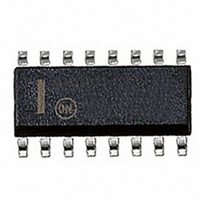
MC33025DWR2 ON Semiconductor, MC33025DWR2 Datasheet - Page 12

MC33025DWR2
Manufacturer Part Number
MC33025DWR2
Description
IC CTRLR PWM HS DBL END 16-SOIC
Manufacturer
ON Semiconductor
Datasheet
1.MC34025DWR2G.pdf
(20 pages)
Specifications of MC33025DWR2
Pwm Type
Voltage/Current Mode
Number Of Outputs
2
Frequency - Max
1MHz
Duty Cycle
45%
Voltage - Supply
10 V ~ 30 V
Buck
No
Boost
No
Flyback
No
Inverting
No
Doubler
No
Divider
No
Cuk
No
Isolated
Yes
Operating Temperature
-40°C ~ 105°C
Package / Case
16-SOIC (0.300", 7.5mm Width)
Frequency-max
1MHz
Duty Cycle (max)
45 %
Output Voltage
5.05 V to 5.15 V
Output Current
500 mA
Mounting Style
SMD/SMT
Switching Frequency
1000 KHz
Operating Supply Voltage
30 V
Maximum Operating Temperature
+ 105 C
Fall Time
30 ns
Minimum Operating Temperature
- 40 C
Rise Time
30 ns
Synchronous Pin
Yes
Topology
Half-Bridge, Push-Pull
Lead Free Status / RoHS Status
Contains lead / RoHS non-compliant
Available stocks
Company
Part Number
Manufacturer
Quantity
Price
Company:
Part Number:
MC33025DWR2G
Manufacturer:
ON
Quantity:
1 000
Part Number:
MC33025DWR2G
Manufacturer:
ON/安森美
Quantity:
20 000
This method of slope compensation is easy to implement, however, it is noise sensitive. Capacitor C
signal is added to the current signal by a voltage divider consisting of resistors R
When only one output is used, this method of slope compensation can be used and it is relatively noise immune. Resistor R
capacitor C
can assume that its charge is linear. First choose C
pulse at the ramp input at the end of every cycle. The charge current I
R
Output
M
= V
CC
/I
M
M
R
.
M
provide the added slope necessary. By choosing R
C
M
Current Sense
Transformer
R
C
R
w
f
f
Figure 30. Current Mode Master/Slave Operation Over Short Distances
Ramp
Input
3
7
Figure 29. Keeps Fig numbering sequence correct
Figure 29A. Slope Compensation (Noise Sensitive)
1.25 V
Figure 29B. Slope Compensation (Noise Immune)
Oscillator
Current Sense
Information
C
M
T
, then R
4
5
6
R
2
http://onsemi.com
M
R
C
C
1
can be adjusted to achieve the required slope. The diode provides a reset
1
T
M
and C
12
4
5
6
7
3
R
M
T
can be calculated by I
V
M
ref
1.25 V
with a larger time constant than the switching frequency, you
Current Sense
Resistor
1
4
5
6
Oscillator
and R
2
.
Oscillator
M
R
f
= C
C
M
Output
1
M
provides AC coupling. The oscillator
S
R
e
C
M
. Then R
f
Ramp
7
3
Input
M
can be calculated by
1.25 V
M
and


