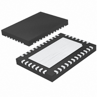
LT3513EUHF#PBF Linear Technology, LT3513EUHF#PBF Datasheet - Page 8

LT3513EUHF#PBF
Manufacturer Part Number
LT3513EUHF#PBF
Description
IC REG 5-OUT FOR TFT-LCD 38QFN
Manufacturer
Linear Technology
Datasheet
1.LT3513EUHFPBF.pdf
(22 pages)
Specifications of LT3513EUHF#PBF
Applications
Converter, TFT, LCD
Voltage - Input
4.5 ~ 30 V
Number Of Outputs
5
Voltage - Output
0.8 ~ 40 V
Operating Temperature
-40°C ~ 125°C
Mounting Type
Surface Mount
Package / Case
38-QFN
Lead Free Status / RoHS Status
Lead free / RoHS Compliant
Available stocks
Company
Part Number
Manufacturer
Quantity
Price
LT3513
pin FuncTions
FB5 (Pin 1): Feedback Pin. Tie the resistor tap to this pin
and set the output of the LDO according to V
(1 + R14/R15). Reference designators refer to Figure 1.
V
Internal Error Amplifier. Connect a series RC from this pin
to ground to compensate switching regulator 1.
RUN-SS3/4 (Pin 3): Run/Soft-Start Pin. This is the soft-
start pin for switching regulators 3 and 4. Place a soft-start
capacitor here to limit start-up inrush current and output
voltage ramp rate. When the BIAS pin reaches 2.25V, a 2µA
current source charges the capacitor. When the voltage at
this pin reaches 0.8V, switches 3 and 4 turn on and begin
switching. For slower start-up use a larger capacitor. For
complete shutdown tie RUN-SS3/4 to ground.
FB3 (Pin 4): Feedback Pin. Tie the resistor tap to this pin
and set V
150mV. Reference designators refer to Figure 1.
RUN-SS2 (Pin 5): Run/Soft-Start Pin. This is the soft-start
pin for switching regulator 2. Place a soft-start capacitor
here to limit start-up inrush current and output voltage
ramp rate. When the BIAS pin reaches 2.25V, a 2µA cur-
rent source charges the capacitor. When the voltage at this
pin reaches 0.8V, switch 2 turns on and begins switching.
For slower start-up use a larger capacitor. For complete
shutdown tie RUN-SS2 to ground.
SW3 (Pin 6): Switch Node. The SW3 pin is the collector of
the internal NPN bipolar transistor for switching regulator 3.
Minimize trace area at this pin to keep EMI down.
E3 (Pin 7): This is switching regulator 3’s output and
the emitter of the output disconnect PNP . Tie the output
capacitor and resistor divider here.
V
regulator 3. V
internal C
V
10% below normal voltage. This output is also disabled
when V
V
by the V
current and when V
8
ONSINK
C1
ON
ON
(Pin 2): Control Voltage and Compensation Pin for
is disabled if any of the four outputs are more than
(Pin 8): This is the delayed output for switching
ON_CLK
ON_CLK
(Pin 9): This is an open-collector output controlled
T
ON
timer times out. Protection circuitry ensures
according to V
ON
pin. When V
is high.
reaches its programmed voltage after the
ON_CLK
ON_CLK
is high, this pin draws current.
ON
= 1.22V • (1 + R8/R9) –
is low, this pin draws no
LDO
= 0.625 •
V
device and the open collector of V
low, the V
impedance. When this pin is high, the V
and the V
PGOOD (Pin 11): Power Good Comparator Output. This is
the open collector output of the power good comparator
and can be used in conjunction with an external P-channel
MOSFET to provide output disconnect for AV
Figure 2. When switcher 2’s output reaches approximately
90% of its programmed voltage, PGOOD will be pulled to
ground. This will pull down on the gate of the MOSFET,
connecting AV
source and the gate of the P-channel MOSFET keeps it
off when switcher 2’s output is low.
V
Internal Error Amplifier. Connect a series RC from this pin
to ground to compensate switching regulator 3.
C
the V
feedback pins reaching 1.125V to V
capacitor value can be set using the equation C = (20µA
• t
GND (Pins 14, 17, 33): Ground.
SW2 (Pins 15, 16): Switch Node. The SW2 pin is the col-
lector of the internal NPN bipolar transistor for switching
regulator 2. Minimize trace area at this pin to keep EMI
down.
BIAS (Pins 18, 29): The BIAS pin is used to improve effi-
ciency when operating at higher input voltages. Connecting
this pin to the output of switching regulator 1 forces most
of the internal circuitry to draw its operating current from
V
4 and the LDO are supplied by BIAS. Switches 2, 3 and 4
and the LDO will not function until the BIAS pin reaches
approximately 2.7V. Both BIAS pins must be tied to V
FB2 (Pin 19): Feedback Pin. Tie the resistor divider tap
to this pin and set AV
(1 + R5/R6). Reference designators refer to Figure 2.
ON_CLK
C3
T
LOGIC
DELAY
(Pin 13): Timing Capacitor Pin. This is the input to
(Pin 12): Control Voltage and Compensation Pin for
ON
rather than V
)/1.1V.
timer and programs the time delay from all four
(Pin 10): This pin controls the output disconnect
ONSINK
ON
pin is enabled and the V
DD
pin sinks current to ground.
. A 100k pull-up resistor between the
IN
. The drivers of switches 2, 3 and
DD
according to AV
ONSINK
ON
ONSINK
turning on. The C
ON
. When this pin is
pin is disabled
DD
DD
pin is a high
as shown in
= 1.22V •
LOGIC
3513fc
T
.


