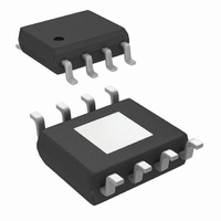
LP2996MR/NOPB National Semiconductor, LP2996MR/NOPB Datasheet - Page 14

LP2996MR/NOPB
Manufacturer Part Number
LP2996MR/NOPB
Description
IC DDR TERMINATION REG 8PSOP
Manufacturer
National Semiconductor
Datasheet
1.LP2996MNOPB.pdf
(18 pages)
Specifications of LP2996MR/NOPB
Applications
Converter, DDR
Voltage - Input
2.2 ~ 5.5 V
Number Of Outputs
1
Operating Temperature
0°C ~ 125°C
Mounting Type
Surface Mount
Package / Case
8-PSOP
Polarity
Positive
Input Voltage Max
5.5 V
Output Voltage
1.159 V, 1.259 V, 1.359 V
Output Type
Fixed
Output Current
1.5 A
Maximum Operating Temperature
+ 125 C
Mounting Style
SMD/SMT
Minimum Operating Temperature
0 C
Reference Voltage
1.358 V
For Use With
LP2996MREVAL - BOARD EVALUATION LP2996MR
Lead Free Status / RoHS Status
Lead free / RoHS Compliant
Voltage - Output
-
Lead Free Status / Rohs Status
Details
Other names
*LP2996MR
*LP2996MR/NOPB
LP2996MR
*LP2996MR/NOPB
LP2996MR
Available stocks
Company
Part Number
Manufacturer
Quantity
Price
Company:
Part Number:
LP2996MR/NOPB
Manufacturer:
SANYO
Quantity:
195
Part Number:
LP2996MR/NOPB
Manufacturer:
NS/国半
Quantity:
20 000
www.national.com
QDR APPLICATIONS
Quad data rate (QDR) applications utilize multiple channels
for improved memory performance. However, this increase in
bus lines has the effect of increasing the current levels re-
quired for termination. The recommended approach in termi-
nating multiple channels is to use a dedicated LP2996 for
each channel. This simplifies layout and reduces the internal
power dissipation for each regulator. Separate V
can be used for each DIMM bank from the corresponding
regulator with the chipset reference provided by a local resis-
This circuit permits termination in a minimum amount of board
space and component count. Capacitor selection can be var-
ied depending on the number of lines terminated and the
maximum load transient. However, with motherboards and
other applications where V
it is advisable to use multiple bulk capacitors and addition to
In most PC applications an extensive amount of decoupling
is required because of the long interconnects encountered
with the DDR-SDRAM DIMMs mounted on modules. As a re-
TT
is distributed across a long plane
FIGURE 14. Typical SSTL-2 Application Circuit for Motherboards
FIGURE 13. Typical SSTL-2 Application Circuit
REF
signals
14
tor divider or one of the LP2996 signals. Because V
V
minor, there should be little difference between the reference
signals of each LP2996.
OUTPUT CAPACITOR SELECTION
For applications utilizing the LP2996 to terminate SSTL-2 I/O
signals the typical application circuit shown in
be implemented.
high frequency decoupling.
an example circuit where 2 bulk output capacitors could be
situated at both ends of the V
Large aluminum electrolytic capacitors are used for their low
ESR and low cost.
sult bulk aluminum electrolytic capacitors in the range of
1000uF are typically used.
TT
are expected to track and the part to part variations are
Figure 12
20057518
TT
20057519
plane for optimal placement.
shown below depicts
Figure 11
REF
and
can


