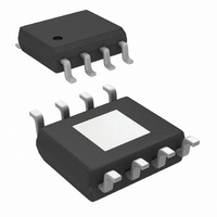
LP2998MR/NOPB National Semiconductor, LP2998MR/NOPB Datasheet - Page 12

LP2998MR/NOPB
Manufacturer Part Number
LP2998MR/NOPB
Description
IC REG TERM VOLT DDRI/II 8-PSOP
Manufacturer
National Semiconductor
Datasheet
1.LP2998MRNOPB.pdf
(18 pages)
Specifications of LP2998MR/NOPB
Applications
Converter, DDR, DDR2, DDR3
Voltage - Input
2.2 ~ 5.5 V
Number Of Outputs
1
Operating Temperature
-40°C ~ 125°C
Mounting Type
Surface Mount
Package / Case
8-PSOP
Primary Input Voltage
2.5V
No. Of Outputs
1
No. Of Pins
8
Output Current
1.5A
Operating Temperature Range
-40°C To +125°C
Msl
MSL 3 - 168 Hours
Filter Terminals
SMD
Rohs Compliant
Yes
For Use With
LP2998EVAL - BOARD EVALUATION FOR LP2998
Lead Free Status / RoHS Status
Lead free / RoHS Compliant
Voltage - Output
-
Other names
LP2998MR
Available stocks
Company
Part Number
Manufacturer
Quantity
Price
Company:
Part Number:
LP2998MR/NOPB
Manufacturer:
TI/NSC
Quantity:
16 500
Part Number:
LP2998MR/NOPB
Manufacturer:
TI/德州仪器
Quantity:
20 000
www.national.com
Typical Application Circuits
Several different application circuits have been shown in
ure 3
are possible in configuring the LP2998. Graphs of the indi-
vidual circuit performance can be found in the Typical Perfor-
mance Characteristics section of the datasheet. These
curves illustrate how the maximum output current is affected
by changes in AVIN and PVIN.
If power dissipation or efficiency is a major concern then the
LP2998 has the ability to operate on split power rails (see
Figure
rail such as 1.8V and the analog circuitry (AVIN) can be con-
nected to a higher rail such as 2.5V, 3.3V or 5V. This allows
the internal power dissipation to be lowered when sourcing
The third option for SSTL-2 applications in the situation that
a 1.8V rail is not available and it is not desirable to use 2.5V,
is to connect the LP2998 power rail to 3.3V (see
this situation AVIN will be limited to operation on the 3.3V or
5V rail as PVIN can never exceed AVIN. This configuration
has the ability to provide the maximum continuous output cur-
through
4). The output stage (PVIN) can be operated on a lower
Figure 12
to illustrate some of the options that
FIGURE 4. Lower Power Dissipation SSTL-2 Implementation
FIGURE 3. Recommended SSTL-2 Implementation
Figure
5). In
Fig-
12
SSTL-2 APPLICATIONS
For the majority of applications that implement the SSTL-2
termination scheme it is recommended to connect all the input
rails to the 2.5V rail. This provides an optimal trade-off be-
tween power dissipation and component count and selection.
An example of this circuit can be seen in
current from V
maximum continuous current is reduced because of the lower
rail voltage, although it is adequate for all motherboard
SSTL-2 applications. Increasing the output capacitance can
also help if periods of large load transients will be encoun-
tered.
rent at the downside of higher thermal dissipation. Care
should be taken to prevent the LP2998 from experiencing
large current levels which cause the device to exceed the
maximum operating junction temperature. Because of this
risk it is not recommended to supply the output stage with a
voltage higher than a nominal 3.3V rail.
TT
. The disadvantage of this circuit is that the
30026910
30026911
Figure
3.


