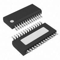
MAX8538EEI+ Maxim Integrated Products, MAX8538EEI+ Datasheet - Page 21

MAX8538EEI+
Manufacturer Part Number
MAX8538EEI+
Description
IC CNTRLR BUCK DUAL 28-QSOP
Manufacturer
Maxim Integrated Products
Datasheet
1.MAX8538EEI.pdf
(23 pages)
Specifications of MAX8538EEI+
Applications
Controller, DDR
Voltage - Input
4.5 ~ 23 V
Number Of Outputs
2
Voltage - Output
0.8 ~ 3.6 V
Operating Temperature
0°C ~ 85°C
Mounting Type
Surface Mount
Package / Case
28-QSOP
Output Voltage
0.8 V to 3.6 V
Output Current
30 A
Input Voltage
4.5 V to 23 V
Mounting Style
SMD/SMT
Maximum Operating Temperature
+ 85 C
Minimum Operating Temperature
- 40 C
Case
SSOP
Dc
05+
Lead Free Status / RoHS Status
Lead free / RoHS Compliant
Case 2: Crossover frequency is greater than the
output-capacitor ESR zero (f
The modulator gain at f
Since the output-capacitor ESR-zero frequency is high-
er than the LC double-pole frequency but lower than
the closed-loop crossover frequency, where the modu-
lator already has -1 slope, the error-amplifier gain must
have zero slope at f
desired -1 slope.
The error-amplifier circuit configuration is the same as
case 1 above; however, the closed-loop crossover fre-
quency is now between f
Figure 7.
The equations that define the error amplifier’s zeros
(f
as case 1; however, f
closed-loop crossover frequency. Therefore, the error-
amplifier gain between f
lated as:
This gain is set by the ratio of R4/R1, where R1 is calcu-
lated in the Output Voltage Setting section. Thus:
Load, Tracking, and DDR Memory Power Supplies
Z1_EA
G
G
Dual-Synchronous Buck Controllers for Point-of-
EA
MOD(FC)
, f
(f
Z1_EA
Z2_EA
f
Z2_EA
) and poles (f
- f
= G
Z2_EA
______________________________________________________________________________________
MOD(DC)
TOP VIEW
/ (f
C
) = G
C
so the loop crosses over at the
P2_EA
Z1_EA
P2_EA
is:
COMP2
REFIN
ILIM2
P2
POK1
POK2
BST2
FREQ
EA(FC)
DH2
x (f
P2_EA
LX2
DL2
EN2
EN1
FB2
SS2
x G
C
and f
and f
P_LC
10
11
12
13
14
is now lower than the
1
2
3
4
5
6
7
8
9
> f
MOD(FC)
, f
x f
Z_ESR
)
P3_EA
P3
Z2_EA
2
MAX8537
MAX8539
Z2_EA
QSOP
/ (f
as illustrated in
Z_ESR
).
) are the same
)
is now calcu-
/ f
P2_EA
x f
28
27
26
25
24
23
22
21
20
19
18
17
16
15
C
BST1
DH1
LX1
ILIM1
PGND
DL1
VL
V+
AVL
VTTR
COMP1
FB1
SS1
GND
)
=
where f
Similar to case 1, C2 can be calculated as:
Set the error-amplifier third pole, f
switching frequency, and let R
The gain of the error amplifier between f
f
G
Similar to case 1, R3, C1, and C3 can be calculated as:
Careful PC board layout is critical to achieve low
switching losses and clean, stable operation. The
switching-power stage requires particular attention.
Follow these guidelines for good PC board layout:
1) Place the decoupling capacitors as close to the IC
P3_EA
EA(FC)
COMP2
ILIM2
POK1
POK2
pins as possible.
BST2
FREQ
DH2
N.C.
LX2
DL2
EN2
EN1
FB2
SS2
10
11
12
13
14
Z2_EA
1
2
3
4
5
6
7
8
9
is set by the ratio of R4/R
R4 = R1 x f
= 1 / G
C3 = C2 / ((2π x C2 x R4 x f
MAX8538
QSOP
= f
C1 = 1 / (2π x R3 x f
MOD(FC)
C2 = 2 / (π x R4 x f
Applications Information
P_LC
R3 = R1 x Ri / (R1 - R
R
I
Z2_EA
PC Board Layout Guidelines
= R4 x G
and f
28
27
26
25
24
23
22
21
20
19
18
17
16
15
. Then:
BST1
DH1
LX1
ILIM1
PGND
DL1
VL
V+
AVL
GND
COMP1
FB1
SS1
GND
/ (f
Pin Configurations
P2_EA
P2_EA
MOD(FC)
I
= (R1 x R3) / (R1 + R3).
= f
P_LC
Z_ESR
x G
Z_ESR
P3_EA
P3_EA
I
I
MOD(FC)
)
and is equal to
)
)
.
) - 1)
, at half the
P2_EA
)
and
21


