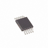
MAX881REUB+ Maxim Integrated Products, MAX881REUB+ Datasheet - Page 5

MAX881REUB+
Manufacturer Part Number
MAX881REUB+
Description
IC SUPPLY BIAS LN 10-UMAX
Manufacturer
Maxim Integrated Products
Datasheet
1.MAX881REUB.pdf
(8 pages)
Specifications of MAX881REUB+
Applications
Charge Pump, Wireless Devices
Voltage - Input
2.5 ~ 5.5 V
Number Of Outputs
1
Voltage - Output
-2V, -2.5 ~ 6.1 V
Operating Temperature
-40°C ~ 85°C
Mounting Type
Surface Mount
Package / Case
10-MSOP, Micro10™, 10-uMAX, 10-uSOP
Function
Inverting
Output Voltage
- 4.9 V to - 0.5 V
Output Current
4 mA (Max)
Supply Current
0.95 mA
Maximum Operating Temperature
+ 85 C
Minimum Operating Temperature
- 40 C
Mounting Style
SMD/SMT
Lead Free Status / RoHS Status
Lead free / RoHS Compliant
Dual Mode is a trademark of Maxim Integrated Products.
Figure 1. Functional Diagram
PIN
10
1
2
3
4
5
6
7
8
9
C1
C2
_______________________________________________________________________________________
NEGOUT
NAME
SHDN
GND
POK
OUT
N.C.
C1+
C1-
FB
IN
NEGOUT
C1+
C1-
0.5V
Positive Terminal for C1
Negative Terminal for C1
Negative Output Voltage (unregulated)
Active-Low, Open-Drain Power-OK Output. Goes low when OUT reaches 92.5% of its set
value.
Active-Low, Logic-Level Shutdown Input. Connect to IN for normal operation. Do not leave this
pin unconnected.
Dual-Mode™ Feedback Input. When FB is connected to GND, the output is preset to -2V. To
select other voltages, connect FB to an external resistor-divider (Figure 4). Do not leave this pin
unconnected.
Regulated Negative Output Voltage
Ground
No Connection. Not internally connected.
Positive Power-Supply Input
CHARGE PUMP
0.4625V
Low-Noise Bias Supply in µMAX
with Power-OK for GaAsFET PA
SHDN
GND
FUNCTION
MAX881R
Pin Description
OUT
POK
FB
IN
C3
C4
5


