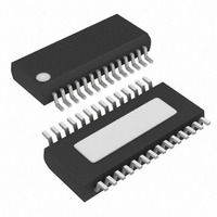
MAX8537EEI+ Maxim Integrated Products, MAX8537EEI+ Datasheet - Page 9

MAX8537EEI+
Manufacturer Part Number
MAX8537EEI+
Description
IC CNTRLR BUCK DUAL 28-QSOP
Manufacturer
Maxim Integrated Products
Datasheet
1.MAX8538EEI.pdf
(23 pages)
Specifications of MAX8537EEI+
Applications
Controller, DDR
Voltage - Input
4.5 ~ 23 V
Number Of Outputs
2
Voltage - Output
0.8 ~ 3.6 V
Operating Temperature
0°C ~ 85°C
Mounting Type
Surface Mount
Package / Case
28-QSOP
Output Voltage
0.8 V to 3.6 V
Output Current
30 A
Input Voltage
4.5 V to 23 V
Mounting Style
SMD/SMT
Maximum Operating Temperature
+ 85 C
Minimum Operating Temperature
- 40 C
Lead Free Status / RoHS Status
Lead free / RoHS Compliant
The MAX8537/MAX8538/MAX8539 step-down DC-DC
converters use a PWM voltage-mode control scheme.
An internal high-bandwidth (25MHz) operational amplifi-
er is used as an error amplifier to regulate the output
voltage. The output voltage is sensed and compared
with an internal 0.8V reference or REFIN to generate an
error signal. The error signal is then compared with a
fixed-frequency ramp by a PWM comparator to give the
appropriate duty cycle to maintain output voltage regula-
tion. At the rising edge of the internal clock, and with DL
(the low-side MOSFET gate drive) at 0V, the high-side
MOSFET turns on. When the ramp voltage reaches the
error-amplifier output voltage, the high-side MOSFET
latches off until the next clock pulse. During the high-
side MOSFET on-time, current flows from the input,
through the inductor, and to the output capacitor and
load. At the moment the high-side MOSFET turns off,
the energy stored in the inductor during the on-time is
released to support the load as the inductor current
ramps down by commutation through the low-side
MOSFET body diode. After a fixed delay, the low-side
MOSFET turns on to shunt the current from its body
diode for lower voltage drop and increased efficiency.
The low-side MOSFET turns off at the rising edge of the
next clock pulse, and when its gate voltage discharges
to zero, the high-side MOSFET turns on and another
cycle starts.
The controllers sense peak inductor current and pro-
vide hiccup-mode overload and short-circuit protection
(see the Current Limit section).
The MAX8537/MAX8538/MAX8539 operate in forced-
PWM mode where the inductor current is always contin-
uous, so even under light load the controller maintains
a constant switching frequency to minimize noise and
possible interference with system circuitry.
Synchronous rectification reduces the conduction loss
in the rectifier by replacing the normal Schottky catch
diode with a low-resistance MOSFET switch. The
MAX8537/MAX8538/MAX8539 controllers also use the
synchronous rectifier to ensure proper startup of the
boost gate-drive circuit.
Gate-drive voltage for the high-side N-channel switch is
generated by a flying-capacitor boost circuit (Figure 1).
The capacitor between BST and LX is alternately
charged from the VL supply and placed in parallel to
the high-side MOSFET’s gate-source terminals.
Load, Tracking, and DDR Memory Power Supplies
Dual-Synchronous Buck Controllers for Point-of-
High-Side Gate-Drive Supply (BST)
Synchronous-Rectifier Driver (DL)
_______________________________________________________________________________________
DC-DC Controller
On startup, the synchronous rectifier (low-side
MOSFET) forces LX to ground and charges the boost
capacitor to VL. On the second half-cycle, the switch-
mode power supply turns on the high-side MOSFET by
closing an internal switch between BST and DH. This
provides the necessary gate-to-source voltage to turn
on the high-side switch, an action that boosts the 5V
gate-drive signal above the input voltage.
All MAX8537/MAX8538/MAX8539 functions are pow-
ered from the on-chip low-dropout 5V regulator with the
input connected to V+. Bypass the regulator’s output
(VL) with a 1µF/10mA or greater ceramic capacitor. The
V+ to VL dropout voltage is typically 500mV, so when
V+ is less than 5.5V, VL is typically (V+ - 500mV).
The internal linear regulator can source up to 70mA to
supply the IC, power the low-side gate drivers, and
charge the external boost capacitors. The current
required to drive the external MOSFETs is calculated as
the total gate charge of the MOSFETs at 5V multiplied
by the switching frequency. At higher frequency, the
MOSFET drive current may exceed the capability of the
internal linear regulator. The output current at VL can
be supplemented with an external PNP transistor as
shown in Figures 4 and 5, which also moves most of
the power dissipation off the IC. The external PNP can
increase the output current at VL to over 200mA. The
dropout voltage increases to 1V (typ).
If VL drops below 3.75V, the MAX8537/MAX8538/
MAX8539 assume that the supply voltage is too low to
make valid decisions, so UVLO circuitry inhibits switch-
ing and forces POK and DH low and DL high. After VL
rises above 4.3V, the controller powers up the outputs
(see the Startup section).
Externally, the MAX8537/MAX8538/MAX8539 start
switching when VL rises above the 4.3V UVLO thresh-
old. However, the controller does not start unless all
four of the following conditions are met: 1) EN_ is high,
2) VL > 4.3V, 3) the internal reference exceeds 80% of
its nominal value (V
limit is not exceeded. Once the MAX8537/MAX8538/
MAX8539 assert the internal enable signal, the con-
troller starts switching and enables soft-start.
Undervoltage Lockout (UVLO)
Internal 5V Linear Regulator
REF
> 0.64V), and 4) the thermal
Startup
9


