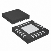
MAX8761ETG+ Maxim Integrated Products, MAX8761ETG+ Datasheet - Page 11

MAX8761ETG+
Manufacturer Part Number
MAX8761ETG+
Description
IC REG LINEAR LCD 24-TQFN
Manufacturer
Maxim Integrated Products
Datasheet
1.MAX8761ETG.pdf
(25 pages)
Specifications of MAX8761ETG+
Applications
Converter, LCD Power Supplies
Voltage - Input
8 ~ 28 V
Number Of Outputs
1
Voltage - Output
5V
Operating Temperature
0°C ~ 85°C
Mounting Type
Surface Mount
Package / Case
24-TQFN Exposed Pad
Lead Free Status / RoHS Status
Lead free / RoHS Compliant
Figures 1, 2, and 3 are the Typical Operating Circuits of
the MAX8710/MAX8761, MAX8711, and MAX8712 for
generating power rails in TFT LCD panels. The input
voltage range is from 10.8V to 13.2V. The AV
is 10V at 300mA, the V
the V
The MAX8710/MAX8711/MAX8712/MAX8761 include a
high-performance linear regulator, a positive charge-
pump regulator, a negative charge-pump regulator, and
built-in power-up sequence control. The MAX8710/
MAX8711/MAX8761 also include a high-current opera-
tional amplifier. Additionally, the MAX8710/MAX8761 pro-
vide logic-controlled high-voltage switches to control the
positive charge-pump output. The linear regulator directly
steps down the input voltage to generate the source-dri-
MAX8710/
MAX8761
18
19
20
21
22
23
24
GOFF
output is -5V at 50mA.
MAX8711
PIN
Typical Operating Circuit
13
14
15
16
—
—
—
______________________________________________________________________________________
Detailed Description
GON
MAX8712
—
10
—
11
12
—
9
output is 27V at 20mA, and
NAME
MODE
SHDN
SRC
CTL
DLP
FBN
FBL
Active-Low Shutdown Control Input. Pull SHDN low to turn off all sections of the
device except REF. Pull SHDN high to enable the device. Cycle SHDN to reset
the device after a fault.
High-Voltage Switch-Control Block Timing Control Input. See the Switch Control
(MAX8710/MAX8761) section for details.
Linear-Regulator Feedback Input. Connect FBL to the center of a resistive
voltage-divider between the linear-regulator output and GND to set the linear-
regulator output voltage. Place the divider within 5mm of FBL.
High-Voltage Switch-Control Block-Mode Selection Input and Timing-Adjustment
Input. See the Switch Control (MAX8710/MAX8761) section for details. MODE is
high impedance when it is connected to REF. MODE is internally pulled to GND
by a 1kΩ resistor during REF UVLO, when V
Positive Charge-Pump Startup Delay and High-Voltage Switch Delay Input.
Connect a capacitor from DLP to GND to set the delay time. A 5µA current
source charges C
shutdown.
Negative Charge-Pump Feedback Input. Connect FBN to the center of a
resistive voltage-divider between the negative output and REF to set the output
voltage. Place the divider within 5mm of FBN. FBN is internally pulled to GND
through a 10Ω resistor in shutdown.
Switch Input. Source of the internal high-voltage p-channel MOSFET connected
to GON.
DD
output
Low-Cost, Linear-Regulator
LCD Panel Power Supplies
ver ICs’ supply voltage. The two built-in charge-pump
regulators are used to generate the TFT gate-on and
gate-off supplies. The high-current operational amplifier is
typically used to drive the LCD backplane (VCOM) and
features high output current (150mA), fast slew rate
(12V/µs), and wide bandwidth (12MHz). Its rail-to-rail
inputs and output maximize flexibility.
The MAX8710/MAX8711/MAX8712/MAX8761 contain a
linear regulator including a PMOS pass transistor. The
MAX8710/MAX8711/MAX8712 can supply an output cur-
rent of at least 300mA and the MAX8761 can supply at
least 500mA. Connect an external resistive voltage-
divider between the regulator output and GND with the
midpoint connected to FBL to adjust the linear-regulator
output. An error amplifier compares the FBL voltage with
the 2.5V internal reference voltage and amplifies the dif-
ference. If the feedback voltage is higher than the
DLP
. DLP is internally pulled to GND by a 10Ω resistor in
Pin Description (continued)
FUNCTION
DLP
< 2.5V, or in shutdown.
Linear Regulator
11


