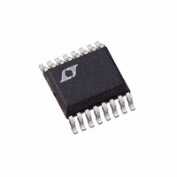
LTC3717EGN Linear Technology, LTC3717EGN Datasheet - Page 8

LTC3717EGN
Manufacturer Part Number
LTC3717EGN
Description
IC STEP-DWN CONTRLR SYNC 16-SSOP
Manufacturer
Linear Technology
Datasheet
1.LTC3717EGN.pdf
(20 pages)
Specifications of LTC3717EGN
Applications
Controller, DDR, QDR
Voltage - Input
4 ~ 36 V
Number Of Outputs
1
Voltage - Output
2 ~ 18 V
Operating Temperature
-40°C ~ 85°C
Mounting Type
Surface Mount
Package / Case
16-SSOP
Lead Free Status / RoHS Status
Contains lead / RoHS non-compliant
Available stocks
Company
Part Number
Manufacturer
Quantity
Price
Part Number:
LTC3717EGN
Manufacturer:
LT/凌特
Quantity:
20 000
Company:
Part Number:
LTC3717EGN#PBF
Manufacturer:
LT
Quantity:
416
Part Number:
LTC3717EGN#TRPBF
Manufacturer:
LT/凌特
Quantity:
20 000
OPERATIO
LTC3717
Main Control Loop
The LTC3717 is a current mode controller for DC/DC
step-down converters. In normal operation, the top
MOSFET is turned on for a fixed interval determined by a
one-shot timer OST. When the top MOSFET is turned off,
the bottom MOSFET is turned on until the current com-
parator I
ating the next cycle. Inductor current is determined by
sensing the voltage between the PGND and SW pins using
the bottom MOSFET on-resistance . The voltage on the I
pin sets the comparator threshold corresponding to in-
ductor valley current. The error amplifier EA adjusts this
I
from the output voltage with a reference equal to 1/3 of the
V
in the feedback voltage relative to the reference. The I
voltage then rises until the average inductor current again
matches the load current. As a result in normal DDR
operation V
The operating frequency is determined implicitly by the
top MOSFET on-time and the duty cycle required to
maintain regulation. The one-shot timer generates an on-
time that is proportional to the ideal duty cycle, thus
holding frequency approximately constant with changes
in V
external resistor R
Overvoltage and undervoltage comparators OV and UV
pull the PGOOD output low if the output feedback voltage
exits a
APPLICATIO S I FOR ATIO
The basic LTC3717 application circuit is shown in
Figure 1. External component selection is primarily deter-
mined by the maximum load current and begins with the
selection of the sense resistance and power MOSFET
switches. The LTC3717 uses the on-resistance of the syn-
chronous power MOSFET for determining the inductor
current. The desired amount of ripple current and operating
frequency largely determines the inductor value. Finally, C
is selected for its ability to handle the large RMS current into
the converter and C
meet the output voltage ripple and transient specification.
8
TH
REF
voltage by comparing 2/3 of the feedback signal V
IN
voltage. If the load current increases, it causes a drop
. The nominal frequency can be adjusted with an
CMP
10% window around the regulation point.
OUT
trips, restarting the one-shot timer and initi-
is equal to 1/2 of the V
U
ON
OUT
U
.
is chosen with low enough ESR to
U
W
REF
voltage.
U
TH
TH
FB
IN
Furthermore, in an overvoltage condition, M1 is turned off
and M2 is turned on and held on until the overvoltage
condition clears.
Pulling the RUN/SS pin low forces the controller into its
shutdown state, turning off both M1 and M2. Releasing
the pin allows an internal 1.2 A current source to charge
up an external soft-start capacitor C
reaches 1.5V, the controller turns on and begins switch-
ing, but with the I
0.6V below the RUN/SS voltage. As C
charge, the soft-start current limit is removed.
INTV
Power for the top and bottom MOSFET drivers and most
of the internal controller circuitry is derived from the
INTV
floating bootstrap capacitor C
charged from INTV
D
pin is grounded, an internal 5V low dropout regulator
supplies the INTV
above 4.7V, the internal regulator is turned off, and an
internal switch connects EXTV
a high efficiency source connected to EXTV
external 5V supply or a secondary output from the
converter, to provide the INTV
7V can be applied to EXTV
the V
undervoltage lockout circuitry prevents the power
switches from turning on.
Maximum Sense Voltage and V
Inductor current is determined by measuring the voltage
across a sense resistance that appears between the PGND
and SW pins. The maximum sense voltage is set by the
voltage applied to the V
mately (0.13)V
sinking current. The current mode control loop will not
allow the inductor current valleys to exceed (0.13)V
R
practice, one should allow some margin for variations in
B
SENSE
when the top MOSFET is turned off. When the EXTV
CC
CC
CC
/EXTV
for sourcing and (0.17)V
pin. The top MOSFET driver is powered from a
voltage is low and INTV
CC
RNG
Power
for sourcing current and (0.17)V
TH
CC
CC
through an external Schottky diode
voltage clamped at approximately
power from V
RNG
CC
pin and is equal to approxi-
for additional gate drive. If
CC
CC
RNG
B
RNG
. This capacitor is re-
to INTV
power. Voltages up to
CC
/R
SS
CC
Pin
drops below 3.4V,
SENSE
. When this voltage
. If EXTV
SS
CC
CC
for sinking. In
continues to
. This allows
, such as an
sn3717 3717fs
CC
RNG
rises
RNG
for
CC
/


