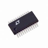
LTC3718EG Linear Technology, LTC3718EG Datasheet - Page 7

LTC3718EG
Manufacturer Part Number
LTC3718EG
Description
IC DC/DC CONTRLR DDR/QDR 24-SSOP
Manufacturer
Linear Technology
Datasheet
1.LTC3718EG.pdf
(20 pages)
Specifications of LTC3718EG
Applications
Controller, DDR, QDR
Voltage - Input
1.5 ~ 36 V
Number Of Outputs
1
Voltage - Output
0.75 ~ 18 V
Operating Temperature
-40°C ~ 85°C
Mounting Type
Surface Mount
Package / Case
24-SSOP
Lead Free Status / RoHS Status
Contains lead / RoHS non-compliant
Available stocks
Company
Part Number
Manufacturer
Quantity
Price
Company:
Part Number:
LTC3718EG
Manufacturer:
LT
Quantity:
2 000
Part Number:
LTC3718EG
Manufacturer:
LT/凌特
Quantity:
20 000
Part Number:
LTC3718EG#PBF
Manufacturer:
LINEAR/凌特
Quantity:
20 000
Company:
Part Number:
LTC3718EG#TRPBF
Manufacturer:
MT
Quantity:
1 255
Part Number:
LTC3718EG#TRPBF
Manufacturer:
LINEAR/凌特
Quantity:
20 000
Company:
Part Number:
LTC3718EGTRPBF
Manufacturer:
LINEAR
Quantity:
594
PI FU CTIO S
RUN/SS (Pin 1): Run Control and Soft-Start Input. A
capacitor to ground at this pin sets the ramp time to full
output current (approximately 3s/ F) and the time delay
for overcurrent latchoff (see Applications Information).
Forcing this pin below 0.8V shuts down the device.
V
the on-time comparator. Tying this pin to the output
voltage makes the on-time proportional to V
comparator input defaults to 0.7V when the pin is grounded,
2.4V when the pin is tied to INTV
PGOOD (Pin 3): Power Good Output. Open-drain logic
output that is pulled to ground when the output voltage of
the buck section is not within 10% of the regulation point.
V
this pin is ten times the nominal sense voltage at maxi-
mum output current and can be set from 0.5V to 2V by a
resistive divider from INTV
defaults to 70mV when this pin is tied to ground, 140mV
when tied to INTV
I
Compensation Point. The current comparator threshold
increases with this control voltage. The voltage ranges
from 0V to 2.4V with 1.2V corresponding to zero sense
voltage (zero current).
SGND (Pins 6, 11): Signal Ground. All small-signal com-
ponents and compensation components should connect to
this ground, which in turn connects to PGND at one point.
I
to this pin to set the one-shot timer current and thereby set
the switching frequency.
V
connects the negative error amplifier input to V
V
Reference voltage for output voltage, power good thresh-
old, and short-circuit shutdown threshold. The output
voltage is set to V
SHDN (Pin 10): Shutdown, Active Low. Tie to 1V or more
to enable boost converter portion of the LTC3718. Ground
to shut down.
TH
ON
ON
RNG
FB1
REF
U
(Pin 5): Current Control Threshold and Error Amplifier
(Pin 7): On-Time Current Input. Tie a resistor from V
(Pin 2): On-Time Voltage Input. Voltage trip point for
(Pin 8): Error Amplifier Feedback Input. This pin
(Pin 9): Positive Input of Internal Error Amplifier.
(Pin 4): Sense Voltage Range Input. The voltage at
U
REF
CC
U
.
/2.
CC
. The nominal sense voltage
CC
.
OUT
OUT
.
. The
IN
V
connected to INTV
voltage on INTV
SW2 (Pin 13): Boost Converter Switch Pin. Connect
inductor/diode for boost converter portion here. Minimize
trace area at this pin to keep EMI down.
PGND (Pins 14, 19): Power Ground. Connect these pins
closely to the source of the bottom N-channel MOSFET,
the (–) terminal of C
V
Portion of LTC3718. Must be locally bypassed.
V
PGND with at least a 1 F ceramic capacitor.
INTV
control circuits are powered from this voltage when V
greater than 5V. Decouple this pin to power ground with a
minimum of 4.7 F low ESR tantalum or ceramic capacitor.
BG (Pin 18): Bottom Gate Drive. Drives the gate of the
bottom N-channel MOSFET between ground and INTV
SENSE
Input. The (–) input to the current comparator is normally
connected to power ground unless using a resistive di-
vider from INTV
SENSE
Input. The (+) input to the current comparator is normally
connected to the SW node unless using a sense resistor
(see Applications Information).
SW1 (Pin 22): Switch Node. The (–) terminal of the
bootstrap capacitor C
from a diode voltage drop below ground up to V
TG (Pin 23): Top Gate Drive. Drives the top N-channel
MOSFET with a voltage swing equal to INTV
posed on the switch node voltage SW.
BOOST (Pin 24): Boosted Floating Driver Supply. The (+)
terminal of the bootstrap capacitor C
pin swings from a diode voltage drop below INTV
V
FB2
IN2
IN1
IN
V
+ INTV
INTVCC
CC
(Pin 12): Boost Converter Feedback. The V
(Pin 16): Main Input Supply. Decouple this pin to
(Pin 15): Input Supply Pin for Boost Converter
–
+
(Pin 17): Internal Regulator Output. The driver and
(Pin 20): Negative Current Sense Comparator
(Pin 21): Positive Current Sense Comparator
CC
= 1.23V(1 + R
.
CC
CC
. Set INTV
CC
(see Applications Information).
VCC
through a resistor divider to set the
B
connects here. This pin swings
and the (–) terminal of C
F2
/R
CC
F1
)
voltage according to:
B
connects here. This
LTC3718
CC
superim-
FB2
IN
CC
IN
.
.
pin is
up to
3718fa
IN
7
CC
is
.


