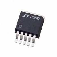
LT1580IQ#TRPBF Linear Technology, LT1580IQ#TRPBF Datasheet - Page 5

LT1580IQ#TRPBF
Manufacturer Part Number
LT1580IQ#TRPBF
Description
IC LDO REGULATOR 7A ADJ DDPKA-5
Manufacturer
Linear Technology
Datasheet
1.LT1580CTPBF.pdf
(16 pages)
Specifications of LT1580IQ#TRPBF
Applications
Converter, Intel Pentium®
Voltage - Input
1.79 ~ 6 V
Number Of Outputs
1
Voltage - Output
1.25 ~ 4.65 V
Operating Temperature
-40°C ~ 125°C
Mounting Type
Surface Mount
Package / Case
D²Pak, TO-263 (5 leads + tab)
Lead Free Status / RoHS Status
Lead free / RoHS Compliant
Available stocks
Company
Part Number
Manufacturer
Quantity
Price
PIN
TYPICAL PERFORMANCE CHARACTERISTICS
SENSE (Pin 1): This pin is the positive side of the reference
voltage for the device. With this pin it is possible to Kelvin
sense the output voltage at the load.
ADJ (Pin 2/5): This pin is the negative side of the
reference voltage for the device. Transient response can
be improved by adding a small bypass capacitor from the
ADJ pin to ground. For fixed voltage devices the ADJ pin
is also brought out to allow the user to add a bypass
capacitor.
GND (Pin 2, 7-Lead Only): For fixed voltage devices this
is the bottom of the resistor divider that sets the output
voltage.
1.258
1.256
1.254
1.252
1.250
1.248
1.246
1.244
1.242
U
–50 –25
LT1580 Reference Voltage
vs Temperature
FUNCTIONS
U
0
TEMPERATURE ( C)
25
50
U
75
(5-Lead/7-Lead)
100
W
125
1580 G04
U
150
2.508
2.506
2.504
2.502
2.500
2.498
2.496
2.494
2.492
–50 –25
LT1580-2.5 Output Voltage
vs Temperature
0
TEMPERATURE ( C)
25
50
V
of the LT1580. The output load current is supplied through
this pin. For the device to regulate, the voltage at this pin
must be between 0.1V and 0.8V greater than the output
voltage (see Dropout specifications).
V
control circuitry of the device. The current flow into this
pin will be about 1% of the output current. For the device
to regulate, the voltage at this pin must be between 1.0V
and 1.3V greater than the output voltage (see Dropout
specifications).
V
POWER
CONTROL
OUT
75
(Pin 3/4): This is the power output of the device.
100
(Pin 5/6): This is the collector to the power device
(Pin 4/3): This pin is the supply pin for the
125
1580 G05
150
LOAD
50mV/DIV
400mA
V
LT1580/LT1580-2.5
OUT
7A
Load Current Step Response
50 s/DIV
1580 TA02
5


