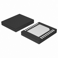
NCP5210MNR2G ON Semiconductor, NCP5210MNR2G Datasheet - Page 8

NCP5210MNR2G
Manufacturer Part Number
NCP5210MNR2G
Description
IC CTLR PWM/DDR DUAL BUCK 20-DFN
Manufacturer
ON Semiconductor
Datasheet
1.NCP5210MNR2G.pdf
(18 pages)
Specifications of NCP5210MNR2G
Applications
Controller, DDR
Voltage - Input
4.5 ~ 13.2 V
Number Of Outputs
3
Operating Temperature
0°C ~ 70°C
Mounting Type
Surface Mount
Package / Case
20-TFQFN Exposed Pad
Output Current
2 A
Switching Frequency
500 KHz
Operating Temperature Range
0 C to + 70 C
Mounting Style
SMD/SMT
Duty Cycle (max)
100 %
Lead Free Status / RoHS Status
Lead free / RoHS Compliant
Voltage - Output
-
Lead Free Status / Rohs Status
Lead free / RoHS Compliant
Other names
NCP5210MNR2G
NCP5210MNR2GOSTR
NCP5210MNR2GOSTR
Available stocks
Company
Part Number
Manufacturer
Quantity
Price
Company:
Part Number:
NCP5210MNR2G
Manufacturer:
MAXIM
Quantity:
68
Part Number:
NCP5210MNR2G
Manufacturer:
ON/安森美
Quantity:
20 000
Channel 2: VDDQ Output Voltage, 1.0 V/div
Channel 3: VTT Output Voltage, 1.0 V/div
Channel 4: V1P5 Output Voltage, 1.0 V/div
Time Base: 5.0 ms/div
Figure 11. VTT Source Current Transient, 0A−2A−0A
Channel 1: Current Sourced out of VTT, 2.0 A/div
Channel 2: VDDQ Output Voltage, AC−Coupled, 100 mV/div
Channel 3: VTT Output Voltage, AC−Coupled, 50 mV/div
Channel 4: V1P5 Output Voltage, AC−Coupled, 100 mV/div
Time Base: 200 ms/div
Figure 9. Power−Up Sequence
TYPICAL OPERATING WAVEFORMS
http://onsemi.com
NCP5210
8
Channel 1: BUF_CUT Pin Voltage, 5.0 V/div
Channel 2: VDDQ Output Voltage, AC−Coupled, 20 mV/div
Channel 3: VTT Output Voltage, AC−Coupled, 100 mV/div
Channel 4: V1P5 Output Voltage, AC−Coupled, 50 mV/div
Time Base: 10 ms/div
Figure 12. VTT Sink Current Transient, 0A−2A−0A
Channel 1: Current Sunk into of VTT, 2.0 A/div
Channel 2: VDDQ Output Voltage, AC−Coupled, 100 mV/div
Channel 3: VTT Output Voltage, AC−Coupled, 50 mV/div
Channel 4: V1P5 Output Voltage, AC−Coupled, 100 mV/div
Time Base: 200 ms/div
Figure 10. S0−S3−S0 Transition


