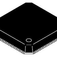
ADP3208DJCPZ-RL ON Semiconductor, ADP3208DJCPZ-RL Datasheet - Page 9

ADP3208DJCPZ-RL
Manufacturer Part Number
ADP3208DJCPZ-RL
Description
IC CTLR BUCK 7BIT 2PHASE 48LFCSP
Manufacturer
ON Semiconductor
Datasheet
1.ADP3208DJCPZ-RL.pdf
(37 pages)
Specifications of ADP3208DJCPZ-RL
Applications
Controller, Power Supplies for Next-Generation Intel Processors
Voltage - Input
3.3 ~ 22 V
Number Of Outputs
1
Voltage - Output
0.01 ~ 1.5 V
Operating Temperature
-10°C ~ 100°C
Mounting Type
Surface Mount
Package / Case
48-LFCSP
Output Voltage
10 mV
Output Current
40 A
Input Voltage
19 V
Supply Current
6 mA
Switching Frequency
300 KHz
Mounting Style
SMD/SMT
Maximum Operating Temperature
+ 100 C
Minimum Operating Temperature
- 10 C
Lead Free Status / RoHS Status
Lead free / RoHS Compliant
Available stocks
Company
Part Number
Manufacturer
Quantity
Price
Company:
Part Number:
ADP3208DJCPZ-RL
Manufacturer:
ON Semiconductor
Quantity:
10
Part Number:
ADP3208DJCPZ-RL
Manufacturer:
ON/安森美
Quantity:
20 000
ELECTRICAL CHARACTERISTICS
= PGND2 = Low = 0 V, EN = VATFREQ = High, DPRSLP = 0 V, PSI = 1.05 V, V
noted (Note 1). Current entering a pin (sunk by the device) has a positive sign. R
DPRSLP
DPRSTP
VARFREQ, SP
EN INPUT
CLKEN OUTPUT
THERMAL MONITORING AND PROTECTION
SUPPLY
HIGH−SIDE MOSFET DRIVER
1. All limits at temperature extremes are guaranteed via correlation using standard Statistical Quality Control (SQC).
2. Guaranteed by design or bench characterization, not production tested.
3. Timing is referenced to the 90% and 10% points, unless otherwise noted.
Input Voltage
Input Current
Input Voltage
Input Current
Input Voltage
Input Current
Input Voltage
Input Current
Output Low Voltage
Output High, Leakage
Current
TTSNS Voltage Range
(Note 2)
TTSNS Threshold
TTSNS Hysteresis
TTSNS Bias Current
VRTT Output Voltage
Supply Voltage Range
Supply Current
V
V
V
Pullup Resistance, Sourcing
Current
Pulldown Resistance, Sinking
Current
CC
CC
CC
OK Threshold
UVLO Threshold
Hysteresis (Note 2)
Parameter
V
Symbol
V
V
CCUVLO
V
CCOK
VRTT
CC
V
CC
= P
VCC1
Refers to driving signal level
Logic low, I
Logic high, I
DPRSLP = low
DPRSLP = high
Refers to driving signal level
Logic low, I
Logic high, I
Refers to driving signal level
Logic low, I
Logic high, I
Refers to driving signal level
Logic low, I
Logic high, I
EN = L or EN = H (Static)
0.8 V < EN < 1.6 V (During Transition)
Logic low, I
Logic high, V
V
TTSNS = 2.6 V
Logic low, I
Logic high, I
EN = H
EN = 0 V
V
V
BST = PVCC
BST = PVCC
CC
CC
CC
= P
= 5.0 V, TTSNS is falling
is Rising
is Falling
http://onsemi.com
VCC2
sink
sink
sink
sink
sink
VRTT(SINK)
source
source
source
source
VRTT(SOURCE)
= BST1 = BST2 = High = 5.0V, FBRTN = GND = SW1 = SW2 = PGND1
CLKEN
= 4 mA
w 1 mA
w 1 mA
w 1 mA
w 1 mA
9
Conditions
v −5 mA
v −5 mA
v −5 mA
v −5 mA
= V
= 400 mA
CC
= −400 mA
VID
REF
= 1.2000 V, T
= 80 kW.
A
= −40°C to 100°C, unless otherwise
2.45
−2.0
Min
2.3
0.7
4.0
2.3
4.0
4.5
4.0
50
0
−1.0
+2.0
Typ
210
110
1.0
1.0
2.5
5.0
6.0
4.3
4.1
1.8
1.0
10
70
50
10
15
Max
2.55
100
100
1.0
0.3
0.7
1.0
1.0
5.0
2.0
5.5
4.5
3.3
3.0
10
50
Unit
mV
mV
mV
mA
mV
mA
mA
mA
nA
mA
mA
mA
mA
W
W
V
V
V
V
V
V
V
V
V
V


