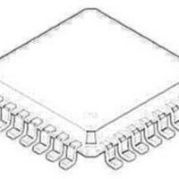
NCP5318FTR2G ON Semiconductor, NCP5318FTR2G Datasheet - Page 29

NCP5318FTR2G
Manufacturer Part Number
NCP5318FTR2G
Description
IC CTLR CPU 2/3/4 PHASE 32-LQFP
Manufacturer
ON Semiconductor
Datasheet
1.NCP5318FTR2G.pdf
(32 pages)
Specifications of NCP5318FTR2G
Applications
Controller, CPU
Voltage - Input
9.5 ~ 13.2 V
Number Of Outputs
4
Operating Temperature
0°C ~ 70°C
Mounting Type
Surface Mount
Package / Case
32-LQFP
Switching Frequency
1 MHz
Mounting Style
SMD/SMT
Primary Input Voltage
18V
No. Of Pins
32
Operating Temperature Range
0°C To +70°C
Termination Type
SMD
Supply Voltage Min
12V
Packaging Type
Tape And Reel
Peak Reflow Compatible (260 C)
Yes
Frequency
1MHz
Rohs Compliant
Yes
Lead Free Status / RoHS Status
Lead free / RoHS Compliant
Voltage - Output
-
Lead Free Status / Rohs Status
Lead free / RoHS Compliant
Other names
NCP5318FTR2G
NCP5318FTR2GOSTR
NCP5318FTR2GOSTR
Available stocks
Company
Part Number
Manufacturer
Quantity
Price
Company:
Part Number:
NCP5318FTR2G
Manufacturer:
ON Semiconductor
Quantity:
10 000
9. Current Sensing
different phases, to limit the maximum phase current and to
limit the maximum system current. Since the current
information is a part of the control loop, better stability is
achieved if the current information is accurate and
noise−free. The NCP5318 uses differential current sense
amplifiers to achieve the best possible performance.
Figure 29.
network (R
Current sensing is used to balance current between
Two sense lines are routed for each phase, as shown in
For inductive current sensing, choose the current sense
constant of the current sense network is too long
Figure 33. V
LOAD CURRENT, 60 A/DIV
(Slow): V
VDRP VOLTAGE,
200 mV/DIV
OUTPUT VOLTAGE,
50 mV/DIV
CSx
200 mS/DIV
, C
R CSx
CSx
DRP
DRP
, x = 1, 2, 3 or 4) to satisfy
and V
tuning waveforms. The RC time
C CSx + Lo
OUT
respond too slowly.
V
constant of the current sense network is optimal:
R L
DRP
Figure 35. V
and V
LOAD CURRENT, 60 A/DIV
OUTPUT VOLTAGE,
50 mV/DIV
VDRP VOLTAGE,
200 mV/DIV
200 mS/DIV
OUT
DRP
without overshooting.
respond to the load current quickly
(eq. 31)
http://onsemi.com
tuning waveforms. The RC time
29
where R
starting point for R
constructed, the value of R
fine−tuned in the lab by observing the V
step change in load current. Tune the R
by varying R
output pin with maximum rise time and minimal overshoot
as shown in Figure 35.
network (R
but maintain the fidelity of the triangular current waveform.
For resistive current sensing, choose the current sense
constant of the current sense network is too short
Figure 34. V
L
is the inductor ESR. This will provide an adequate
(Fast): V
CSx
OUTPUT VOLTAGE, 50 mV/DIV
LOAD CURRENT, 60 A/DIV
CSx
, C
VDRP VOLTAGE,
500 mV/DIV
CSx
to provide a “square−wave” at the V
DRP
200 mS/DIV
DRP
CSx
, x = 1, 2, 3, or 4) to reject noise spikes,
tuning waveforms. The RC time
and V
and C
CSx
OUT
CSx
(and/or C
both overshoot.
. After the converter is
CSx
DRP
x C
CSx
signal during a
CSx
) should be
network
DRP


