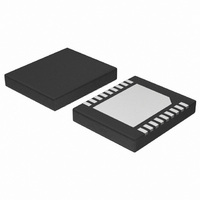
NCP5220MNR2G ON Semiconductor, NCP5220MNR2G Datasheet - Page 14

NCP5220MNR2G
Manufacturer Part Number
NCP5220MNR2G
Description
IC CTLR PWM DUAL BUCK PWR 20-DFN
Manufacturer
ON Semiconductor
Datasheet
1.NCP5220MNR2G.pdf
(18 pages)
Specifications of NCP5220MNR2G
Applications
Controller, DDR
Voltage - Input
5 ~ 12 V
Number Of Outputs
2
Operating Temperature
0°C ~ 70°C
Mounting Type
Surface Mount
Package / Case
20-TFDFN
Switching Frequency
250 KHz
Operating Temperature Range
0 C to + 70 C
Mounting Style
SMD/SMT
Duty Cycle (max)
100%
Lead Free Status / RoHS Status
Lead free / RoHS Compliant
Voltage - Output
-
Lead Free Status / Rohs Status
Lead free / RoHS Compliant
Other names
NCP5220MNR2G
NCP5220MNR2GOSTR
NCP5220MNR2GOSTR
Available stocks
Company
Part Number
Manufacturer
Quantity
Price
Company:
Part Number:
NCP5220MNR2G
Manufacturer:
SIPEX
Quantity:
4 100
Application Circuit
application circuit for NCP5220. The NCP5220 is
specifically designed as a total power solution for the MCH
and DDR memory system. This diagram contains NCP5220
for driving four external N−Ch FETs to form the DDR
memory supply voltage (VDDQ) and the MCH regulator.
Output Inductor Selection
ripple current with transient response capability. A value of
1.7 mH will yield about 3.0 A peak−peak ripple current when
converting from 5.0 V to 2.5 V at 250 kHz. It is important
that the rated inductor current is not exceeded during full
load, and that the saturation current is not less than the
expected peak current. Low ESR inductors may be required
to minimize DC losses and temperature rise.
Input Capacitor Selection
provide a stable, low impedance source node for the buck
regulator to convert from. The usual practice is to use a
combination of electrolytic capacitors and multi−layer
ceramic capacitors to provide bulk capacitance and high
frequency noise suppression. It is important that the
capacitors are rated to handle the AC ripple current at the
input of the buck regulators, as well as the input voltage. In
the NCP5220 the DDQ and MCH regulators are interleaved
(out of phase by 180 degrees) to reduce the peak AC input
current.
Output Capacitor Selection
the requirements for low output ripple voltage and transient
voltage. Low ESR electrolytic capacitors can be effective at
reducing ripple voltage at 250 kHz. Low ESR ceramic
capacitors are most effective at reducing output voltage
excursions caused by fast load steps of system memory and
the memory controller.
Figure 20, on the following page, shows the typical
The value of the output inductor is chosen by balancing
Input capacitors for PWM power supplies are required to
Output capacitors are chosen by balancing the cost with
NCP5220
COMP_1P5
GND_1P5
SW_DDQ
BG_DDQ
TG_DDQ
5VDUAL
BG_1P5
SLP_S3
TG_1P5
BOOT
20
19
18
17
16
15
14
13
12
11
TP2
12VATX
5VDUAL
Figure 19. Charge Pump Circuit at BOOT Pin
D2
BAT54HT1
4.7
1 k
4.7
R2
R3
R4
APPLICATION INFORMATION
BAT54HT1
1
1
D2
4
3
4
3
Q2
NTD40N03
DPAK
Q2
NTD40N03
http://onsemi.com
NCP5220
14
5VDUAL
Power MOSFET Selection
the requirements for the current load of the memory system
and the efficiency of the converter provided. The selections
criteria can be based on drain−source voltage, drain current,
on−resistance R
R
preferred to achieve the high current requirement of the
DDR memory system and MCH, as well as the high
efficiency of the converter. The tradeoff is a corresponding
increase in the input gate capacitor of the power MOSFETs.
PCB Layout Considerations
more of current. It is very important to use wide traces or
large copper shapes to carry current from the input node
through the MOSFET switches, inductor and to the output
filters and load. Reducing the length of high current nodes
will reduce losses and reduce parasitic inductance. It is
usually best to locate the input capacitors the MOSFET
switches and the output inductor in close proximity to
reduce DC losses, parasitic inductance losses and radiated
EMI.
networks should be placed near the NCP5220 and away
from the switch nodes and other noisy circuit elements.
Placing compensation components near each other will
minimize the loop area and further reduce noise
susceptibility.
Optional Boost Voltage Configuration
of boost voltage scheme of Figure 20. The advantage in
Figure 19 is the elimination of the requirement for the Zener
clamp.
DS(on)
Power MOSFETs are chosen by balancing the cost with
With careful PCB layout the NCP5220 can supply 20 A or
The sensitive voltage feedback and compensation
The charge pump circuit in Figure 19 can be used instead
TP2
C4
100 nF
D1
BAT54HT1
L
and high drain current power MOSFETs are usually
VDDQ
C6
4.7
mF
DS(on)
+
and input gate capacitance. Low
C7
2200
mF
+
C25
2200
mF
R15
1 k
2.5 VDDQ
TP5


