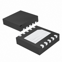
MAX8794ETB+T Maxim Integrated Products, MAX8794ETB+T Datasheet - Page 12

MAX8794ETB+T
Manufacturer Part Number
MAX8794ETB+T
Description
IC DDR LINEAR REG 10-TDFN
Manufacturer
Maxim Integrated Products
Datasheet
1.MAX8794ETBT.pdf
(13 pages)
Specifications of MAX8794ETB+T
Applications
Converter, DDR
Voltage - Input
1.1 ~ 3.6 V
Number Of Outputs
1
Voltage - Output
0.5 ~ 1.5 V
Operating Temperature
-40°C ~ 85°C
Mounting Type
Surface Mount
Package / Case
10-TDFN Exposed Pad
Lead Free Status / RoHS Status
Lead free / RoHS Compliant
The MAX8794 operates with low-dropout voltage and
low quiescent current in notebook computers while
maintaining good noise, transient response, and AC-
rejection specifications. Improved supply-noise rejec-
tion and transient response can be achieved by
increasing the values of the input and output capaci-
tors. Use passive filtering techniques when operating
from noisy sources.
The MAX8794 load-transient response graphs (see the
Typical Operating Characteristics ) show two compo-
nents of the output response: a DC shift from the output
impedance due to the load-current change and the
transient response. A typical transient response for a
step change in the load current from -1.5A to +1.5A is
10mV. Increasing the output capacitor’s value and
decreasing the ESR attenuate the overshoot.
Low-Voltage DDR Linear Regulator
TRANSISTOR COUNT: 3496
PROCESS: BiCMOS
12
______________________________________________________________________________________
Noise, PSRR, and Transient Response
Chip Information
The MAX8794 requires proper layout to achieve the
intended output power level and low noise. Proper lay-
out involves the use of a ground plane, appropriate
component placement, and correct routing of traces
using appropriate trace widths. Refer to the MAX8794
evaluation kit for a layout example:
1) Minimize high-current ground loops. Connect the
2) To optimize performance, a ground plane is essen-
3) Connect the input filter capacitor less than 10mm
4) Connect the backside pad to a large ground plane.
For the latest package outline information and land patterns, go
to www.maxim-ic.com/packages. Note that a “+”, “#”, or “-” in
the package code indicates RoHS status only. Package draw-
ings may show a different suffix character, but the drawing per-
tains to the package regardless of RoHS status.
PACKAGE TYPE
ground of the device, the input capacitor, and the
output capacitor together at one point.
tial. Use all available copper layers in applications
where the device is located on a multilayer board.
from IN. The connecting copper trace carries large
currents and must be at least 2mm wide, preferably
5mm wide.
Use as much copper as necessary to decrease the
thermal resistance of the device. In general, more
copper provides better heatsinking capabilities.
10 TDFN-EP
PACKAGE CODE
Package Information
T1033+1
PCB Layout Guidelines
DOCUMENT NO.
21-0137


