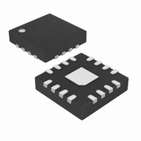
MAX8506ETE+T Maxim Integrated Products, MAX8506ETE+T Datasheet

MAX8506ETE+T
Specifications of MAX8506ETE+T
Related parts for MAX8506ETE+T
MAX8506ETE+T Summary of contents
Page 1
... REF 0.22µF HP Typical Application Circuits continued at end of data sheet. ________________________________________________________________ Maxim Integrated Products For pricing, delivery, and ordering information, please contact Maxim/Dallas Direct! at 1-888-629-4642, or visit Maxim’s website at www.maxim-ic.com. ♦ Integrated 75mΩ (typ) Bypass FET ♦ 38mV Dropout at 600mA Load ♦ ...
Page 2
PWM Step-Down DC-DC Converters with 75m Ω Ω Bypass FET for WCDMA and cdmaOne Handsets ABSOLUTE MAXIMUM RATINGS SHDN, SKIP, HP, REFIN, BATTP, BATT, OUT GND ...........................................................-0.3V to +6V PGND to GND .......................................................-0.3V to +0.3V BATT to BATTP......................................................-0.3V ...
Page 3
PWM Step-Down DC-DC Converters with 75m Ω Ω Bypass FET for WCDMA and cdmaOne Handsets ELECTRICAL CHARACTERISTICS (continued) = 3.6V, SHDN = SKIP = BATT GND BATT BATTP C = 0.22µ -40°C ...
Page 4
PWM Step-Down DC-DC Converters with 75m Ω Ω Bypass FET for WCDMA and cdmaOne Handsets = 3.6V, SHDN = SKIP = BATT GND BATT BATTP EFFICIENCY vs. OUTPUT VOLTAGE IN NORMAL MODE 100 R ...
Page 5
PWM Step-Down DC-DC Converters with 75m Ω Ω Bypass FET for WCDMA and cdmaOne Handsets = 3.6V, SHDN = SKIP = BATT GND BATT BATTP LIGHT-LOAD SWITCHING WAVEFORM IN PWM MODE V = 0.4V ...
Page 6
PWM Step-Down DC-DC Converters with 75m Ω Ω Bypass FET for WCDMA and cdmaOne Handsets PIN NAME MAX8506 MAX8508 MAX8507 SHDN GND 3 3 REF 4 — REFIN 5 5 COMP ...
Page 7
PWM Step-Down DC-DC Converters with 75m Ω Ω Bypass FET for WCDMA and cdmaOne Handsets The MAX8506/MAX8507/MAX8508 use a fixed-frequen- cy, current-mode and PWM controller capable of achiev- ing 100% duty cycle. Current-mode feedback provides cycle-by-cycle current limiting and superior ...
Page 8
PWM Step-Down DC-DC Converters with 75m Ω Ω Bypass FET for WCDMA and cdmaOne Handsets Synchronous Rectification An N-channel synchronous rectifier operates during the second half of each switching cycle (off-time). When the inductor current falls below the N-channel current- ...
Page 9
PWM Step-Down DC-DC Converters with 75m Ω Ω Bypass FET for WCDMA and cdmaOne Handsets Table 1. Suggested Inductors PART SUPPLIER NUMBER Murata LQH32C-53 Sumida CDRH2D11 Taiyo Yuden LBLQ2016 TOKO D312C capacitor ripple. This sets the device speed for transient ...
Page 10
PWM Step-Down DC-DC Converters with 75m Ω Ω Bypass FET for WCDMA and cdmaOne Handsets Typical Application Circuits (MAX8508) (continued) INPUT 2.6V TO 5.5V 2.2µF SKIP SHDN REF 0.22µF 1MHz OSC HP TOP VIEW SHDN 1 GND 2 REF 3 ...
Page 11
... Maxim cannot assume responsibility for use of any circuitry other than circuitry entirely embodied in a Maxim product. No circuit patent licenses are implied. Maxim reserves the right to change the circuitry and specifications without notice at any time. Maxim Integrated Products, 120 San Gabriel Drive, Sunnyvale, CA 94086 408-737-7600 ____________________ 11 © 2004 Maxim Integrated Products Printed USA is a registered trademark of Maxim Integrated Products ...


