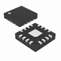
MAX8508ETE+T Maxim Integrated Products, MAX8508ETE+T Datasheet - Page 9

MAX8508ETE+T
Manufacturer Part Number
MAX8508ETE+T
Description
IC DC-DC CONV PWM 16-TQFN
Manufacturer
Maxim Integrated Products
Datasheet
1.MAX8506ETET.pdf
(11 pages)
Specifications of MAX8508ETE+T
Applications
Converter, WCDMA
Voltage - Input
2.6 ~ 5.5 V
Number Of Outputs
1
Voltage - Output
0.75 ~ 3.4 V
Operating Temperature
-40°C ~ 85°C
Mounting Type
Surface Mount
Package / Case
16-TQFN Exposed Pad
Lead Free Status / RoHS Status
Lead free / RoHS Compliant
capacitor ripple. This sets the device speed for transient
response and allows the use of small ceramic output
capacitors because the phase-shifted capacitor ripple
does not disturb the current-regulation loop. The resistor
sets the proportional gain of the output error voltage by
a factor of g
es the sensitivity of the control loop to output ripple.
The resistor and capacitor set a compensation zero that
defines the system’s transient response. The load cre-
ates a dynamic pole, shifting in frequency with changes
in load. As the load decreases, the pole frequency
shifts to the left. System stability requires that the com-
pensation zero must be placed to ensure adequate
phase margin (at least 30° at unity gain). With a 4.7µF
output capacitor, the recommended C
MAX8506 are 1500pF and 10kΩ, respectively. This pro-
vides adequate phase margin over the entire output
voltage and load range and optimizes the output-
voltage settling time for REFIN dynamic control. See the
Typical Application Circuits for recommended C
R
A 4µH to 6µH inductor is recommended for most appli-
cations. For best efficiency, the inductor’s DC resistance
should be <400mΩ. Saturation current (I
greater than the maximum DC load at the PA’s supply
plus half the inductor current ripple. Two-step V
applications typically require very small inductors with
I
for recommended inductors and suppliers.
Table 1. Suggested Inductors
SAT
Bypass FET for WCDMA and cdmaOne Handsets
Murata
Sumida
Taiyo Yuden
TOKO
C
values for the MAX8507 and MAX8508.
in the 200mA to 300mA region. See Tables 1 and 2
PWM Step-Down DC-DC Converters with 75m Ω Ω
SUPPLIER
m
x R
C
_______________________________________________________________________________________
. Increasing this resistor also increas-
LQH32C-53
CDRH2D11
LBLQ2016
NUMBER
D312C
PART
Inductor Selection
C
SAT
and R
INDUCTANCE
) should be
(µH)
4.7
4.7
4.7
4.7
C
for the
C
and
CC
ESR (mΩ)
High switching frequencies and large peak currents
make PC board layout a very important part of design.
Good design minimizes EMI, noise on the feedback
paths, and voltage gradients in the ground plane, all of
which can result in instability or regulation errors.
Connect the inductor, input filter capacitor, and output fil-
ter capacitor as close together as possible and keep their
traces short, direct, and wide. The external voltage- feed-
back network should be very close to the FB pin, within
0.2in (5mm). Keep noisy traces, such as those from the
LX pin, away from the voltage-feedback network. Position
the bypass capacitors as close as possible to their
respective supply and ground pins to minimize noise cou-
pling. For optimum performance, place input and output
capacitors as close to the device as possible. Connect
GND directly under the IC to the exposed paddle. Refer
to the MAX8506 evaluation kit for an example PC board
layout and routing scheme.
Table 2. Component Suppliers
Murata
Sumida
Taiyo Yuden
TOKO
150
135
250
200
SUPPLIER
SATURATION
CURRENT (A)
PC Board Layout and Routing
0.650
0.500
0.210
0.790
770-436-1300
847-956-0666
408-573-4150
847-297-0070
PHONE
DIMENSIONS (mm)
www.murata.com
www.sumida.com
www.t-yuden.com
www.tokoam.com
2.5 x 3.2 x 1.7
3.2 x 3.2 x 1.2
1.6 x 2.0 x 1.6
3.6 x 3.6 x 1.2
WEBSITE
9


