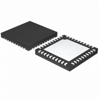
MAX1567ETL+T Maxim Integrated Products, MAX1567ETL+T Datasheet - Page 27

MAX1567ETL+T
Manufacturer Part Number
MAX1567ETL+T
Description
IC DGTL CAM PWR-SUP 6CH 40TQFN
Manufacturer
Maxim Integrated Products
Datasheet
1.MAX1567ETLT.pdf
(35 pages)
Specifications of MAX1567ETL+T
Applications
Controller, Digital Camera
Voltage - Input
0.7 ~ 5.5 V
Number Of Outputs
7
Voltage - Output
1.25 ~ 5 V
Operating Temperature
-40°C ~ 85°C
Mounting Type
Surface Mount
Package / Case
40-TQFN Exposed Pad
Lead Free Status / RoHS Status
Lead free / RoHS Compliant
up may have difficulty starting into heavy loads (see the
Minimum Startup Voltage vs. Load Current (OUTSU)
graph in the Typical Operating Characteristics); however,
this can be remedied by connecting an external P-
channel load switch driven by SCF so the load is not
connected until the PVSU is in regulation (Figure 17).
The step-up converter is activated with a high input at
ONSU. The main converter (step-up or step-down) is acti-
vated by a high input on ONM. The step-down and auxil-
iary DC-to-DC converters 1, 2, and 3 activate with high
inputs at ONSD, ON1, ON2, and ON3, respectively. The
step-down, main, and AUX_ converters cannot be activat-
ed until PVSU is in regulation. For automatic startup, con-
nect ON_ to PVSU or a logic level greater than 1.6V.
Choose a switching frequency to optimize external
component size or circuit efficiency for the particular
application. Typically, switching frequencies between
400kHz and 500kHz offer a good balance between
component size and circuit efficiency—higher frequen-
cies generally allow smaller components, and lower fre-
quencies give better conversion efficiency. The
switching frequency is set with an external timing resis-
tor (R
cycle, the timing capacitor charges through the resistor
until it reaches V
where C
the OSC pin due to internal ESD protection structure
and the die-to-package capacitance.
The internal comparator that compares the capacitor
C
(typ). The capacitor voltage then decays to zero over
time, t
f
between 22pF and 470pF. Determine R
See the Typical Operating Characteristics for f
R
All MAX1566/MAX1567 output voltages are resistor set.
The FB_ threshold is 1.25V for all channels except for
FB3L (0.2V) on both devices and FB2 (inverter) on the
MAX1567. When setting the voltage for any channel
OSC
OSC
OSC
t
1
= -R
OSC
can be set from 100kHz to 1MHz. Choose C
2
using different values of C
voltage to the reference has a delay t
= 200ns. The oscillator frequency is as follows:
par
) and capacitor (C
OSC
R
OSC
(15pF typ) is the parasitic capacitance at
Setting the Switching Frequency
x (C
REF
f
= (200ns + 50ns - 1/ f
OSC
OSC
______________________________________________________________________________________
([C
. The charge time, t
= 1 / (t
OSC
+ C
Setting Output Voltages
+ C
par
Design Procedure
OSC
1
Six-Channel, High-Efficiency, Digital
) x ln (1 - 1.25 / V
+ t
par
). At the beginning of a
OSC
d
] ln[1 - 1.25 / V
+ t
.
2
)
OSC
OSC
1
, is as follows:
Shutdown
) /
:
d
PVSU
PVSU
OSC
of 50ns
OSC
)
])
vs.
Camera Power Supplies
except the MAX1567 AUX2, connect a resistive volt-
age-divider from the channel output to the correspond-
ing FB_ input and then to GND. The FB_ input bias
current is less than 100nA, so choose the bottom-side
(FB_-to-GND) resistor to be 100kΩ or less. Then calcu-
late the top-side (output-to-FB_) resistor:
When using AUX3 to drive white LEDs (Figure 7), select
the LED current-setting resistor (R3, Figure 7) using the
following formula:
The FB2 threshold on the MAX1567 is 0V. To set the
AUX2 negative output voltage, connect a resistive volt-
age-divider from the negative output to the FB2 input,
and then to REF. The FB2 input bias current is less than
100nA, so choose the REF-side (FB2-to-REF) resistor
(R
(output-to-FB2) resistor:
The input capacitor in a DC-to-DC converter reduces
current peaks drawn from the battery or other input
power source and reduces switching noise in the con-
troller. The impedance of the input capacitor at the
switching frequency should be less than that of the
input source so high-frequency switching currents do
not pass through the input source.
The output capacitor keeps output ripple small and
ensures control-loop stability. The output capacitor must
also have low impedance at the switching frequency.
Ceramic, polymer, and tantalum capacitors are suitable,
with ceramic exhibiting the lowest ESR and high-frequen-
cy impedance.
Output ripple with a ceramic output capacitor is
approximately as follows:
If the capacitor has significant ESR, the output ripple
component due to capacitor ESR is as follows:
Output capacitor specifics are also discussed in each
converter’s Compensation section.
This section describes component selection for the
step-up, as well as for the main, if SUSD = PV.
The external components required for the step-up are
an inductor, an input and output filter capacitor, and a
compensation RC.
REF
) to be 100kΩ or less. Then calculate the top-side
V
RIPPLE
R
R
General Filter Capacitor Selection
TOP
TOP
V
RIPPLE(ESR)
= I
= R
Step-Up Component Selection
= R
L(PEAK)
BOTTOM
R3 = 0.2V / I
REF
(-V
[1 / (2π x f
= I
OUT(AUX2)
[(V
L(PEAK)
OUT
LED
/ 1.25) - 1]
OSC
x ESR
/ 1.25)
x C
OUT
)]
27


