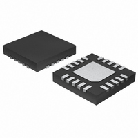
MAX1543ETP+T Maxim Integrated Products, MAX1543ETP+T Datasheet - Page 16

MAX1543ETP+T
Manufacturer Part Number
MAX1543ETP+T
Description
IC DC-DC CONV TFT-LCD 20-TQFN
Manufacturer
Maxim Integrated Products
Datasheet
1.MAX1543ETP.pdf
(20 pages)
Specifications of MAX1543ETP+T
Applications
Controller, TFT, LCD
Voltage - Input
2.6 ~ 5.5 V
Number Of Outputs
2
Voltage - Output
2.6 ~ 13 V
Operating Temperature
-40°C ~ 85°C
Mounting Type
Surface Mount
Package / Case
20-TQFN Exposed Pad
Lead Free Status / RoHS Status
Lead free / RoHS Compliant
TFT LCD DC-to-DC Converter with
Operational Amplifiers
operating point (η
in the Typical Operating Characteristics:
Calculate the ripple current at that operating point and
the peak current required for the inductor:
The inductor’s saturation current rating and the
MAX1542/MAX1543s’ LX current limit (I
exceed I
should exceed I
choose an inductor with less than 0.5Ω series resis-
tance.
Considering the Typical Application Circuits, the maxi-
mum load current (I
output and a typical input voltage of 3.3V.
Choosing an LIR of 0.6 and estimating efficiency of
85% at this operating point:
Using the circuit’s minimum input voltage (2.7V) and
estimating efficiency of 80% at that operating point,
The ripple current and the peak current are:
The total output voltage ripple has two components: the
capacitive ripple caused by the charging and dis-
charging of the output capacitance, and the ohmic rip-
ple due to the capacitor’s equivalent series resistance
(ESR):
where I
Inductor Selection section). For ceramic capacitors, the
output voltage ripple is typically dominated by V
PLE(C)
tics of the output capacitor must also be considered.
16
I
I
RIPPLE
IN(DC,MAX)
I
L = (3.3V)
RIPPLE
I
IN(DC,MAX)
______________________________________________________________________________________
. The voltage rating and temperature characteris-
1.2MHz) = 4.7µH
I
PEAK
PEAK
= 2.7V
= 317mA
PEAK
V
V
V
= V
I
RIPPLE
RIPPLE ESR
RIPPLE C
PEAK
V
2 ✕
= I
IN(MIN)
MAIN
= 741mA + (317mA / 2) = 900mA
is the peak inductor current (see the
= (0.2A
and the inductor’s DC current rating
0.85
MAIN(MAX)
✕
IN(DC,MAX)
= I
(
( )
(8V - 2.7V) / (4.7µH
=
MIN
)
IN(DC,MAX)
V
Output Capacitor Selection
≅
RIPPLE ESR
✕
✕
) taken from an appropriate curve
MAIN(MAX)
)
C
I
(8V - 3.3V) / ((8V)
≅
(V
MAIN
✕
OUT
I
PEAK
MAIN
8V / (2.7V
✕
(
. For reasonable efficiency,
V
MAIN
V
-V
+ (I
x R
)
MAIN
V
) is 200mA with an 8V
IN(MIN)
+
MAIN
V
RIPPLE
ESR COUT
RIPPLE C
/ (V
✕
× ƒ
0.8)) = 741mA
✕
(
−
IN(MIN)
) / (L
1.2MHz
V
OSC
2 ✕
IN
) / 2
( )
LIM
0.6
)
✕
,
and
f
✕
) should
OSC
✕
✕
η
0.2A
8V)
MIN
✕
RIP-
)
✕
The input capacitor (C
drawn from the input supply and reduces noise injec-
tion into the device. A 10µF ceramic capacitor is used
in the Typical Application Circuits (Figures 1 and 2)
because of the high source impedance seen in typical
lab setups. Actual applications usually have much
lower source impedance since the step-up regulator
often runs directly from the output of another regulated
supply. Typically, C
used in the Typical Application Circuits. Ensure a low-
noise supply at IN by using adequate C
The MAX1542/MAX1543 operate with an adjustable out-
put from V
to FB (Typical Application Circuits) from the output
(V
where V
1.24V. Since the input bias current into FB is typically
zero, R
ing accuracy, although lower values provide better
noise immunity. Connect the resistor-divider as close to
the IC as possible.
Choose R
gain for fast transient response. Choose C
the integrator zero to maintain loop stability.
For low-ESR output capacitors, use the following equa-
tions to obtain stable performance and good transient
response:
To further optimize transient response, vary R
20% steps and C
transient response waveforms.
For highest efficiency, always choose the lowest num-
ber of charge-pump stages that meet the output
requirements. Figures 5 and 6 show the positive and
MAIN
Selecting the Number of Charge-Pump Stages
) to AGND. Select the resistor values as follows:
2
FB
can have a value up to 100kΩ without sacrific-
R
C
COMP
IN
, the step-up converter feedback set point, is
COMP
COMP
to 13V. Connect a resistive voltage-divider
≅
≅
to set the high-frequency integrator
COMP
R
500
IN
10
1
=
can be reduced below the values
Input Capacitor Selection
R
x I
x V
IN
2
in 50% steps while observing
L x I
) reduces the current peaks
MAIN MAX
V
IN
V
OUT
MAIN
V
FB
Loop Compensation
x V
MAIN MAX
(
x C
OUT
−
(
1
)
Output Voltage
OUT
Charge Pumps
x R
x C
IN
)
COMP
.
OUT
COMP
COMP
to set
in


