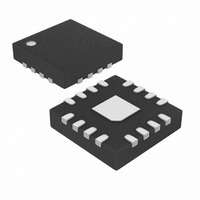
MAX8723ETE+T Maxim Integrated Products, MAX8723ETE+T Datasheet - Page 15

MAX8723ETE+T
Manufacturer Part Number
MAX8723ETE+T
Description
IC REG FOR LCD DISPLAY 16-TQFN
Manufacturer
Maxim Integrated Products
Specifications of MAX8723ETE+T
Applications
Converter, LCD
Voltage - Input
6 ~ 13.2 V
Number Of Outputs
1
Voltage - Output
3.3V, 2 ~ 3.6 V
Operating Temperature
-40°C ~ 85°C
Mounting Type
Surface Mount
Package / Case
16-TQFN Exposed Pad
Lead Free Status / RoHS Status
Lead free / RoHS Compliant
To improve efficiency, an external synchronous rectifier
MOSFET can be driven by EXT. When this MOSFET is
used, the Schottky diode’s current rating can be
reduced or the diode can be omitted entirely. Choose a
MOSFET with low R
pulled up by the internal high-side switch turning on
due to parasitic drain-to-gate capacitance, causing
cross-conduction problems. Switching losses are not
an issue for the synchronous rectifier in the step-down
topology, since it is a zero-voltage switched device.
The MAX8723 has a built-in power MOSFET switch and
gate-driver circuits. Although the step-down regulator
operates with high efficiency, inevitably the IC internal
power circuits consume some power and heat the IC
up, especially under heavy-load conditions. To ensure
the best performance of the silicon, thermal manage-
ment is critical in the application.
The built-in low-side MOSFET is not dedicated for syn-
chronous rectifier application and has high on-resis-
tance. An external freewheeling device such as
Schottky diode or MOSFET is essential for the circuit
operation. Without this freewheeling device, the heat
generated by the built-in low-side MOSFET imperils the
MOSFET and the IC operation, especially under heavy-
load conditions such as 2A load.
The TQFN package provides an exposed metal pad on
the MAX8723 backside. This back pad also serves as
heat sink to the internal silicon circuitry, as well as a
ground substrate. Soldering the exposed backside pad
to a large copper plane on PC board can significantly
help to dissipate heat generated inside the IC.
Typically, the large copper plane is not available on the
component side of PC board. Place a large solder pad
under the IC with multiple vias connecting to a large
ground plane on another board layer and solder the IC
exposed back pad to this solder pad.
Good layout is necessary to achieve the MAX8723’s
intended output power level, high efficiency, and low
noise. Good layout includes the use of ground planes,
careful component placement, and correct routing of
traces using appropriate trace widths. The following
points are in order of decreasing importance:
PC Board Layout and Grounding
Applications Information
______________________________________________________________________________________
DS(ON).
Low-Cost, Internal-Switch, Step-Down
Thermal Considerations
Ensure that EXT is not
External MOSFET
Regulator for LCD Displays
1) Minimize switched-current and high-current ground
2) Connect the input filter capacitor less than 5mm
3) Connect high-current loop components with short,
4) Place the LX node components as close together
5) Place feedback voltage-divider resistors as close to
6) Minimize the length and maximize the width of the
7) Ground planes are essential for optimum perfor-
Refer to the MAX8723 evaluation kit for an example of
proper board layout.
loops. Connect the input capacitor’s ground, the out-
put capacitor’s ground, and PGND together with
short, wide traces or a small ground plane. Connect
the resulting island to GND at only one point.
away from IN. Place INL pin and REF pin bypass
capacitors as close to the device as possible, no
more than 5mm. The ground connection of the INL
bypass capacitor should be connected directly to
the GND pin with a wide trace.
wide connections. Avoid using vias in the high-cur-
rent paths. If vias are unavoidable, use many vias in
parallel to reduce resistance and inductance. The
connecting copper trace carries large currents and
must be at least 1mm wide, preferably 2.5mm.
and as near to the device as possible. Minimize the
length of the LX node while keeping it wide and
short. This reduces resistive and switching losses,
as well as noise. Keep the LX node away from FB
feedback node and analog ground. Use inner layers
etc., as shield if necessary.
the FB feedback pin as possible. The divider’s cen-
ter trace should be kept short. Placing the resistors
far away causes the FB traces to become antennas
that can pick up switching noise. Care should be
taken to avoid running any feedback trace near LX.
traces between the output capacitors and the load
for best transient responses.
mance. In most applications, the circuit is located on
a multilayer board and full use of the four or more
layers is recommended. For heat dissipation, con-
nect the exposed backside pad to a large analog
ground plane, preferably on a surface of the board
that receives good airflow. If the ground is not locat-
ed on the IC component side of PC board, use multi-
ple vias to the IC backside pad to lower thermal
resistance. Typical applications use multiple ground
planes to reduce thermal resistance. Avoid large AC
currents through the analog ground plane.
15


