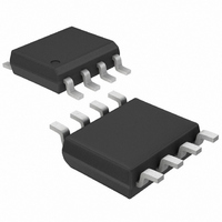
MAX607ESA+ Maxim Integrated Products, MAX607ESA+ Datasheet - Page 11

MAX607ESA+
Manufacturer Part Number
MAX607ESA+
Description
IC DC-DC CONVERT 8-SOIC
Manufacturer
Maxim Integrated Products
Datasheet
1.MAX606ESA.pdf
(12 pages)
Specifications of MAX607ESA+
Applications
Converter, Flash Memory PCMCIA Cards
Voltage - Input
3 ~ 5.5 V
Number Of Outputs
1
Voltage - Output
12V, 3 ~ 12.5 V
Operating Temperature
0°C ~ 85°C
Mounting Type
Surface Mount
Package / Case
8-SOIC (3.9mm Width)
Lead Free Status / RoHS Status
Lead free / RoHS Compliant
The MAX606/MAX607’s high switching frequency
demands a high-speed rectifier. Use a Schottky diode
with at least a 0.5A average current rating and a 1.2A
peak current rating, such as an MBR0520L. See Table
3 for a list of component suppliers.
The output voltage ripple is a function of the output
capacitor’s equivalent series resistance (ESR) and
capacitance. For best performance, use ceramic
capacitors. Higher-ESR capacitors, such as tantalums,
will cause excessive ripple. See Table 3 for a list of
component suppliers.
The output voltage ripple is approximately 100mVp-p
for the 12V Standard Application Circuit (Figure 1) and
50mV for the 5V circuit (Figure 2). To further reduce this
ripple, or to reduce the ripple on a different application
circuit, increase the value of the output filter capacitor.
If this capacitor is low ESR (e.g., ceramic), the output
voltage ripple will be dominated by this capacitance.
For applications where the MAX606/MAX607 are physi-
cally close to the input supply’s filter capacitor (e.g., in
PCMCIA drivers from the host computer), the input
bypass capacitor may not be necessary.
In other applications where the MAX606/MAX607 are
more than a few inches away from the supply (such as
memory cards), the input bypass capacitor is needed
to reduce reflected current ripple to the supply and
improve efficiency by creating a low-impedance path
for the ripple current. Under these circumstances, the
associated high Q and low ESR of ceramic capacitors
do not diminish the problem. Therefore, include some
low-Q, moderate-ESR capacitance (e.g., tantalum) at
the input in order to reduce ringing.
The MAX606/MAX607’s high-frequency operation and
high peak currents make PC board layout critical to
minimize ground bounce and noise. Locate input
bypass and output filter capacitors as close to the
device pins as possible. All connections to OUT (and to
FB when operating in adjustable-output mode) should
also be kept as short as possible. A ground plane is
recommended. Solder GND and PGND directly to the
ground plane. Refer to the MAX606/MAX607 evaluation
kit manual for a suggested surface-mount layout.
DC-DC Converters for Flash Memory/PCMCIA Cards
______________________________________________________________________________________
Low-Profile, 5V/12V or Adjustable, Step-Up
Input Bypass Capacitors
Capacitor Selection
Output Filter Capacitor
Diode Selection
Layout
TRANSISTOR COUNT: 613
SUBSTRATE CONNECTED TO GND
___________________Chip Topography
PGND
PGND
PGND
SHDN
SEL
V+
(1.473mm)
0.058"
LX
LX
LX
OUT
SS
GND
(2.134mm)
0.084"
11


