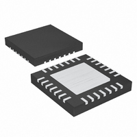
MAX8550AETI+ Maxim Integrated Products, MAX8550AETI+ Datasheet - Page 18

MAX8550AETI+
Manufacturer Part Number
MAX8550AETI+
Description
IC PWR SUP DDR INTEG 28TQFN
Manufacturer
Maxim Integrated Products
Datasheet
1.MAX8550AETIT.pdf
(29 pages)
Specifications of MAX8550AETI+
Applications
Controller, DDR
Voltage - Input
2 ~ 28 V
Number Of Outputs
2
Voltage - Output
1.8V, 2.5V, 0.7 ~ 5.5 V
Operating Temperature
-40°C ~ 85°C
Mounting Type
Surface Mount
Package / Case
28-TQFN Exposed Pad
Output Voltage
0.7 V to 5.5 V, 1.8 V, 2.5 V
Output Current
1.5 A
Input Voltage
2 V to 28 V
Mounting Style
SMD/SMT
Maximum Operating Temperature
+ 85 C
Minimum Operating Temperature
- 40 C
Lead Free Status / RoHS Status
Lead free / RoHS Compliant
• Maximum Load Current. There are two values to con-
• Switching Frequency. This choice determines the
• Inductor Operating Point. This choice provides trade-
The MAX8550A dual-mode operation allows the selec-
tion of common voltages without requiring external
components (Figure 5). Connect FB to GND for a fixed
2.5V output, to AV
FB directly to OUT for a fixed 0.7V output.
The buck-regulator output voltage can be adjusted from
0.7V to 5.5V using a resistive voltage-divider (Figure 6).
The MAX8550A regulates FB to a fixed reference volt-
age (0.7V). The adjusted output voltage is:
Integrated DDR Power-Supply Solution for
Desktops, Notebooks, and Graphic Cards
18
sider. The peak load current (I
instantaneous component stresses and filtering
requirements and thus drives output capacitor selec-
tion, inductor saturation rating, and the design of the
current-limit circuit. The continuous load current
(I
drives the selection of input capacitors, MOSFETs,
and other critical heat-contributing components.
basic trade-off between size and efficiency. The opti-
mal frequency is largely a function of maximum input
voltage, due to MOSFET switching losses proportion-
al to frequency and V
also a moving target due to rapid improvements in
MOSFET technology that are making higher frequen-
cies more practical.
offs: size vs. efficiency and transient response vs. out-
put ripple. Low inductor values provide better
transient response and smaller physical size but also
result in lower efficiency and higher output ripple due
to increased ripple currents. The minimum practical
inductor value is one that causes the circuit to operate
at the edge of critical conduction (where the inductor
current just touches zero with every cycle at maximum
load). Inductor values lower than this grant no further
size-reduction benefit. The optimum operating point is
usually found between 20% and 50% ripple current.
When pulse skipping (SKIP = low at light loads), the
inductor value also determines the load-current value
at which PFM/PWM switchover occurs.
LOAD
Setting the Buck Regulator Output (V
______________________________________________________________________________________
) determines the thermal stresses and thus
V
Setting the Output Voltage (Buck)
OUT
=
DD
V
FB
for a fixed 1.8V output, or connect
Resistive Voltage-Divider at FB
⎛
⎜
⎝
IN
1
2
+
. The optimum frequency is
R
R
Preset Output Voltages
D
C
⎞
⎟ +
⎠
PEAK
V
RIPPLE
) determines the
2
OUT
) with a
where V
and V
The termination power-supply output (VTT) can be set by
two different methods. First, the VTT output can be con-
nected directly to the VTTS input to force VTT to regulate
to V
higher than V
from VTT to VTTS. The maximum value for VTT is V
V
= +85°C.
The termination reference voltage (VTTR) tracks 1/2
V
The switching frequency and inductor operating point
determine the inductor value as follows:
For example: I
2.5V, f
Figure 5. Dual-Mode Feedback Decoder
DROPOUT
REFIN
Setting the VTT and VTTR Voltages (LDO)
REF (2.0V)
REFIN
0.1V
RIPPLE
FB
SW
.
L
FB
L
V
= 600kHz, 30% ripple current or LIR = 0.3:
RIPPLE
=
/ 2. Secondly, VTT can be forced to regulate
=
where V
is 0.7V, R
is:
12
REFIN
V
AMPLIFIER
IN
LOAD(MAX)
V
ERROR
=
×
×
2 5
TO
/ 2 by connecting a resistive divider
DROPOUT
LIR
.
V
600
f
SW
OUT
C
V
Inductor Selection (Buck)
and R
(
kHz
×
12
×
I
(
V
LOAD MAX
= 12A, V
V
I
LOAD MAX
IN
×
- 2.5V)
= I
D
12
-
(
are shown in Figure 6,
VTT
V
(
A
OUT
MAX8550A
×
× 0.3Ω (max) at T
IN
)
)
)
0 3
×
= 12V, V
×
.
R
LIR
≈
ESR
1
μ
H
OUT
(FIXED)
(FIXED)
VTTI
1.8V
2.5V
OUT
=
A
-


