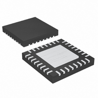
MAX8744ETJ+ Maxim Integrated Products, MAX8744ETJ+ Datasheet - Page 25

MAX8744ETJ+
Manufacturer Part Number
MAX8744ETJ+
Description
IC CNTRLR PWR SUP QUAD 32TQFN
Manufacturer
Maxim Integrated Products
Datasheet
1.MAX8745ETJT.pdf
(36 pages)
Specifications of MAX8744ETJ+
Applications
Controller, Notebook Computers
Voltage - Input
6 ~ 26 V
Number Of Outputs
4
Voltage - Output
3.3V, 5V, 1 ~ 26 V
Operating Temperature
0°C ~ 85°C
Mounting Type
Surface Mount
Package / Case
32-TQFN Exposed Pad
Duty Cycle (max)
99 %
Output Voltage
3.315 V, 5.015 V, 2 V to 5.5 V
Mounting Style
SMD/SMT
Switching Frequency
200 KHz, 300 KHz, 500 KHz
Maximum Operating Temperature
+ 85 C
Minimum Operating Temperature
- 40 C
Synchronous Pin
No
Topology
Boost, Flyback, Forward
Lead Free Status / RoHS Status
Lead free / RoHS Compliant
ON3, ON5, or SHDN to clear the fault latch and restart
the SMPS controllers.
Each SMPS controller includes an output UVP protec-
tion circuit that begins to monitor the output 6144 clock
cycles (1/f
high). If either SMPS output voltage drops below 70% of
its nominal regulation voltage and the UVP protection is
enabled, the UVP circuit sets the fault latch, pulls
PGOOD low, and shuts down both controllers using the
soft-shutdown sequence. When an SMPS output voltage
drops to 0.1V, its synchronous rectifier turns on, clamp-
ing the discharged output to GND. Cycle LDO5 below
1V or toggle either ON3, ON5, or SHDN to clear the fault
latch and restart the SMPS controllers.
The MAX8744/MAX8745 feature a thermal fault-protec-
tion circuit. When the junction temperature rises above
+160°C, a thermal sensor activates the fault latch, pulls
PGOOD low, and shuts down both SMPS controllers
using the soft-shutdown sequence. When an SMPS out-
put voltage drops to 0.1V, its synchronous rectifier
turns on, clamping the discharged output to GND.
Toggle either ON3, ON5, or SHDN to clear the fault
latch and restart the controllers after the junction tem-
perature cools by 15°C.
The MAX8744/MAX8745 include an auxiliary linear regu-
lator (OUTA) that can be configured for 12V, ideal for
PCMCIA power requirements, and for biasing the gates
of load switches in a portable device. OUTA can also be
configured for outputs from 1V to 23V. The auxiliary regu-
lator has an independent ON/OFF control, allowing it to
be shut down when not needed, reducing power con-
sumption when the system is in a low-power state.
A flyback-winding control loop regulates a secondary
winding output, improving cross-regulation when the pri-
mary output is lightly loaded or when there is a low input-
output differential voltage. If V
low-side switch is turned on for a time equal to 33% of
the switching period. This reverses the inductor (primary)
current, pulling current from the output filter capacitor
and causing the flyback transformer to operate in for-
ward mode. The low impedance presented by the trans-
former secondary in forward mode dumps current into
the secondary output, charging up the secondary
capacitor and bringing V
tion. The secondary feedback loop does not improve
secondary output accuracy in normal flyback mode,
where the main (primary) output is heavily loaded. In this
condition, secondary output accuracy is determined by
Supply Controllers for Notebook Computers
OSC
Auxiliary LDO Detailed Description
High-Efficiency, Quad-Output, Main Power-
) after that output is enabled (ON_ pulled
Output Undervoltage Protection (UVP)
______________________________________________________________________________________
INA
< V
Thermal Fault Protection
OUTA
DRVA
back into regula-
< V
OUTD
, the
the secondary rectifier drop, transformer turns ratio, and
accuracy of the main output voltage.
Firmly establish the input voltage range and maximum
load current before choosing a switching frequency
and inductor operating point (ripple-current ratio). The
primary design trade-off lies in choosing a good switch-
ing frequency and inductor operating point, and the fol-
lowing four factors dictate the rest of the design:
•
•
•
•
Input Voltage Range. The maximum value
(V
AC-adapter voltage. The minimum value (V
must account for the lowest battery voltage after
drops due to connectors, fuses, and battery selector
switches. If there is a choice at all, lower input volt-
ages result in better efficiency.
Maximum Load Current. There are two values to
consider. The peak load current (I
determines the instantaneous component stresses
and filtering requirements and thus drives output
capacitor selection, inductor saturation rating, and
the design of the current-limit circuit. The continu-
ous load current (I
stresses and thus drives the selection of input
capacitors, MOSFETs, and other critical heat-con-
tributing components.
Switching Frequency. This choice determines the
basic trade-off between size and efficiency. The opti-
mal frequency is largely a function of maximum input
voltage, due to MOSFET switching losses that are
proportional to frequency and V
quency is also a moving target, due to rapid improve-
ments in MOSFET technology that are making higher
frequencies more practical.
Inductor Operating Point. This choice provides
trade-offs between size vs. efficiency and transient
response vs. output ripple. Low inductor values pro-
vide better transient response and smaller physical
size, but also result in lower efficiency and higher out-
put ripple due to increased ripple currents. The mini-
mum practical inductor value is one that causes the
circuit to operate at the edge of critical conduction
(where the inductor current just touches zero with
every cycle at maximum load). Inductor values lower
than this grant no further size-reduction benefit. The
optimum operating point is usually found between
20% and 50% ripple current. When pulse skipping
(SKIP low and light loads), the inductor value also
determines the load-current value at which
PFM/PWM switchover occurs.
IN(MAX)
) must accommodate the worst-case, high
SMPS Design Procedure
LOAD
) determines the thermal
IN
2
. The optimum fre-
LOAD(MAX)
IN(MIN)
25
)
)


