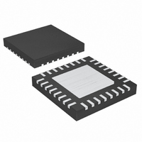
MAX17004ETJ+ Maxim Integrated Products, MAX17004ETJ+ Datasheet - Page 32

MAX17004ETJ+
Manufacturer Part Number
MAX17004ETJ+
Description
IC PS CTRLR FOR NOTEBOOKS 32TQFN
Manufacturer
Maxim Integrated Products
Datasheet
1.MAX17003ETJ.pdf
(36 pages)
Specifications of MAX17004ETJ+
Applications
Controller, Notebook Computers
Voltage - Input
6 ~ 26 V
Number Of Outputs
4
Voltage - Output
3.3V, 5V, 2 ~ 5.5 V
Operating Temperature
-40°C ~ 85°C
Mounting Type
Surface Mount
Package / Case
32-TQFN Exposed Pad
Lead Free Status / RoHS Status
Lead free / RoHS Compliant
where Q
high-side MOSFET’s data sheet. For example, assume
the FDS6612A n-channel MOSFET is used on the high
side. According to the manufacturer’s data sheet, a sin-
gle FDS6612A has a maximum gate charge of 13nC
(V
boost capacitance would be:
Selecting the closest standard value, this example
requires a 0.1µF ceramic capacitor.
Adjust the auxiliary linear regulator’s output voltage by
connecting a resistive divider between OUTA and ana-
log ground with the center tap connected to FBA
(Figure 1). Select R6 in the 10kΩ to 30kΩ range, and
calculate R5 with the following equation:
where V
The pass transistor must meet specifications for current
gain (β), input capacitance, collector-emitter saturation
voltage, and power dissipation. The transistor’s current
gain limits the guaranteed maximum output current to:
where I
rent, V
and R
High-Efficiency, Quad-Output, Main Power-
Supply Controllers for Notebook Computers
32
GS
______________________________________________________________________________________
= 5V). Using the above equation, the required
BE
BE
DRV
FBA
GATE
is the base-to-emitter voltage of the transistor,
is the pullup resistor connected between the
I
LOAD MAX
is the minimum guaranteed base drive cur-
= 1.0V.
C
is the total gate charge specified in the
BST
(
R
LDOA Design Procedure
5
C
=
=
BST
)
R
200
13
Output Voltage Selection
=
6
⎛
⎜
⎝
⎛
⎜
⎝
=
nC
mV
V
I
DRV
V
OUTA
Q
200
FBA
GATE
Transistor Selection
=
−
mV
0 065
R
V
.
−
BE
BE
1
⎞
⎟
⎠
⎞
⎟
⎠
μ
β
F
MIN
transistor’s base and emitter. Furthermore, the transis-
tor’s current gain increases the linear regulator’s DC
loop gain (see the LDOA Stability Requirements sec-
tion), so excessive gain destabilizes the output.
Therefore, transistors with current gain over 100 at the
maximum output current can be difficult to stabilize and
are not recommended. The transistor’s input capaci-
tance and input resistance also create a second pole,
which could be low enough to make the output unsta-
ble when heavily loaded.
The transistor’s saturation voltage at the maximum out-
put current determines the minimum input-to-output
voltage differential that the linear regulator supports.
Alternatively, the package’s power dissipation could
limit the useable maximum input-to-output voltage dif-
ferential. The maximum power-dissipation capability of
the transistor’s package and mounting must exceed the
actual power dissipation in the device. The power dissi-
pation equals the maximum load current times the max-
imum input-to-output differential:
The MAX17003/MAX17004 linear-regulator controller
uses an internal transconductance amplifier to drive an
external pnp pass transistor. The transconductance
amplifier, the pass transistor, the base-to-emitter resistor,
and the output capacitor determine the loop stability.
The transconductance amplifier regulates the output
voltage by controlling the pass transistor’s base cur-
rent. The total DC loop gain is approximately:
where V
transistor’s DC gain, and I
the base-to-emitter resistor (R
emitter resistor used in Figure 1 was chosen to provide
a 1mA bias current (I
T
is 26mV at room temperature, h
PWR = I
A
V LDO
(
PWR = I
LDOA Stability Requirements
)
LOAD(MAX)
=
BIAS
⎛
⎜
⎝
5 5
V
LOAD(MAX)
.
T
).
V
BIAS
⎞
⎟
⎠
⎛
⎜
⎝
1
(V
+
BE
INA
is the current through
I
BIAS FE
). The 680Ω base-to-
I
LOAD
V
- V
CE
h
OUTA
⎞
⎟
⎠
FE
)
is the pass


