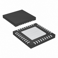
MAX8720ETX+ Maxim Integrated Products, MAX8720ETX+ Datasheet - Page 23

MAX8720ETX+
Manufacturer Part Number
MAX8720ETX+
Description
IC CNTRL VID STP DWN 36-TQFN
Manufacturer
Maxim Integrated Products
Datasheet
1.MAX8720ETXT.pdf
(31 pages)
Specifications of MAX8720ETX+
Applications
Controller, CPU GPU
Voltage - Input
2 ~ 28 V
Number Of Outputs
1
Voltage - Output
0.28 ~ 1.85 V
Operating Temperature
0°C ~ 85°C
Mounting Type
Surface Mount
Package / Case
36-TQFN Exposed Pad
Output Voltage
0.275 V to 1.85 V
Input Voltage
2 V to 28 V
Mounting Style
SMD/SMT
Maximum Operating Temperature
+ 85 C
Minimum Operating Temperature
- 40 C
Lead Free Status / RoHS Status
Lead free / RoHS Compliant
If the MAX8720 is configured for pulse-skipping opera-
tion (SKIP = GND) when SUS goes high, the MAX8720
immediately enters forced-PWM mode, ramping the
output voltage down to the S0, S1 programmed voltage
at the slew rate determined by R
blanks PGOOD (forced high impedance) until the tran-
sition is completed plus 8 extra R
internal target voltage equals the selected S0, S1 DAC
voltage. After this blanking time expires, the controller
enters pulse-skipping operation.
When exiting suspend mode (SUS pulled low), the
MAX8720 immediately enters forced-PWM mode and
ramps the output up at the slew rate set by R
controller blanks PGOOD (forced high impedance) until
the transition is completed plus 8 extra R
the internal target voltage equals the selected D0–D5
DAC voltage. After this blanking time expires, the con-
troller returns to pulse-skipping operation.
The overvoltage-protection (OVP) circuit is designed to
protect the CPU against a shorted high-side MOSFET
by drawing high current and blowing the battery fuse.
The output voltage is continuously monitored for over-
voltage. If the output is more than 2.25V, OVP is trig-
gered and the circuit shuts down. The DL low-side
gate-driver output is then latched high until SHDN is
toggled or V
turns on the synchronous-rectifier MOSFET with 100%
duty and, in turn, rapidly discharges the output filter
capacitor and forces the output to ground. If the condi-
tion that caused the overvoltage (such as a shorted
high-side MOSFET) persists, the battery fuse blows. DL
is also kept high continuously in shutdown when V
above the UVLO threshold.
The output UVP function is similar to foldback current
limiting, but employs a timer rather than a variable cur-
rent limit. If the MAX8720 output voltage is under 70%
of the nominal value, the PWM is latched off and won’t
restart until V
To allow startup, UVP is ignored until the internal DAC
reaches the final target plus 8 extra R
UVP can be defeated through the no-fault test mode
(see the No-Fault Test Mode section).
The over/undervoltage-protection features can compli-
cate the process of debugging prototype breadboards
since there are (at most) a few milliseconds in which to
CC
CC
Output Undervoltage Shutdown
Output Overvoltage Protection
power is cycled below 1V. This action
Suspend Transition (Pulse-Skipping
power is cycled or SHDN is toggled.
______________________________________________________________________________________
No-Fault Test Mode
Operation Selected)
TIME
Dynamically Adjustable 6-Bit VID
TIME
TIME
. The controller
TIME
clocks.
clocks—the
TIME
clocks—
CC
. The
is
determine what went wrong. Therefore, a test mode is
provided to disable the OVP, UVP, and thermal-shut-
down features, and clear the fault latch if it has been
set. The no-fault test mode is entered by forcing 12V to
15V on SHDN.
Firmly establish the input voltage range and maximum
load current before choosing a switching frequency
and inductor operating point (ripple-current ratio). The
primary design trade-off lies in choosing a good switch-
ing frequency and inductor operating point, and the fol-
lowing four factors dictate the rest of the design:
• Input Voltage Range. The maximum value
• Maximum Load Current. There are two values to
• Switching Frequency. This choice determines the
• Inductor Operating Point. This choice provides
(V
AC-adapter voltage. The minimum value (V
must account for the lowest battery voltage after
drops due to connectors, fuses, and battery selector
switches. If there is a choice at all, lower input volt-
ages result in better efficiency.
consider. The peak load current (I
mines the instantaneous component stresses and fil-
tering requirements and thus drives output-capacitor
selection, inductor saturation rating, and the design of
the current-limit circuit. The continuous load current
(I
ves the selection of input capacitors, MOSFETs, and
other critical heat-contributing components.
basic trade-off between size and efficiency. The
optimal frequency is largely a function of maximum
input voltage, due to MOSFET switching losses that
are proportional to frequency and V
mum frequency is also a moving target, due to rapid
improvements in MOSFET technology that are mak-
ing higher frequencies more practical.
trade-offs between size vs. efficiency, and transient
response vs. output ripple. Low inductor values pro-
vide better transient response and smaller physical
size, but also result in lower efficiency and higher
output ripple due to increased ripple currents. The
minimum practical inductor value is one that causes
the circuit to operate at the edge of critical conduc-
tion (where the inductor current just touches zero
with every cycle at maximum load). Inductor values
lower than this grant no further size-reduction benefit.
The optimum operating point is usually found
between 20% and 50% ripple current. When pulse
skipping (SKIP low and light loads), the inductor
Step-Down Controller
LOAD
IN(MAX)
) determines the thermal stresses and thus dri-
) must accommodate the worst-case, high
Design Procedure
LOAD(MAX)
IN
2
. The opti-
IN(MIN)
) deter-
23
)


