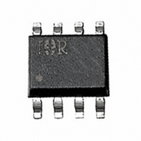
IRU3033CS International Rectifier, IRU3033CS Datasheet - Page 3

IRU3033CS
Manufacturer Part Number
IRU3033CS
Description
IC CTRL/REG PWM SWITCH 8-SOIC
Manufacturer
International Rectifier
Datasheet
1.IRU3033CSTR.pdf
(12 pages)
Specifications of IRU3033CS
Applications
Controller, Intel Pentium®, II, P55C
Voltage - Input
12V
Number Of Outputs
1
Voltage - Output
2 ~ 3.5 V
Operating Temperature
0°C ~ 70°C
Mounting Type
Surface Mount
Package / Case
8-SOIC (3.9mm Width)
Lead Free Status / RoHS Status
Contains lead / RoHS non-compliant
Other names
*IRU3033CS
IRU3033-CS
IRU3033-CS
IRU3033-CS
IRU3033-CS
Available stocks
Company
Part Number
Manufacturer
Quantity
Price
Part Number:
IRU3033CS
Manufacturer:
IR
Quantity:
20 000
Part Number:
IRU3033CSDTR
Manufacturer:
IR
Quantity:
20 000
Part Number:
IRU3033CSTR
Manufacturer:
IR
Quantity:
20 000
PIN DESCRIPTIONS
PIN #
BLOCK DIAGRAM
1
2
3
4
5
6
7
8
Drv 1
Gnd
1
5
PIN SYMBOL
V
V
Drv1
Gnd
Drv2
V
V
12(SW)
V
V
HYST
FB1
FB2
12
12(SW)
2
The PWM output of the switching controller. This pin is a totem pole drive that is con-
nected to the gate of the power MOSFET. A resistor may be placed from this pin to the
gate in order to reduce switching noise.
This pin supplies the voltage to the PWM drive and hysteresis circuitry and it is connected
to the 12V supply. A 1µF, high frequency capacitor must be connected from this pin to
ground to provide the peak current for charging and discharging of the MOSFET.
A resistor divider from this pin to the output of the switching regulator and ground sets the
Core supply voltage.
A resistor and a 10pF capacitor is connected from this pin to the V
ripple voltage for the switching regulator.
This pin is connected to the IC substrate and must be connected to the lowest potential in
the system.
The feedback pin of the linear regulator. A resistor divider from this pin to the output of the
linear regulator and ground sets the I/O supply voltage.
The drive pin of the linear regulator. This pin controls the base of a transistor or the gate
of a MOSFET acting as the series pass element for the linear regulator.
This pin provides the biasing for the chip and drive for the linear regulator controller. It is
connected to 12V supply. A 10Ω resistor in series from this pin to the 12V supply and a
1µF, high frequency capacitor connected from this pin to ground is required to filter the
switching noise of the switching regulator.
V
PIN DESCRIPTION
HYST
4
Figure 2 - Simplified block diagram of the IRU3033.
PWM Control
UVLO
www.irf.com
V
FB1
3
1.25V
V
REF
5V Reg
V
IRU3033(PbF)
8
12
FB1
pin to set the output
Drv2
V
FB2
7
6
3


