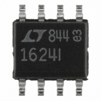
LTC1624IS8#PBF Linear Technology, LTC1624IS8#PBF Datasheet - Page 8

LTC1624IS8#PBF
Manufacturer Part Number
LTC1624IS8#PBF
Description
IC SW REG CONTROLLER N-CH 8-SOIC
Manufacturer
Linear Technology
Type
Step-Down (Buck), Step-Up (Boost), Inverting, Sepicr
Datasheet
1.LTC1624CS8PBF.pdf
(28 pages)
Specifications of LTC1624IS8#PBF
Internal Switch(s)
No
Synchronous Rectifier
No
Number Of Outputs
1
Voltage - Output
1.19 ~ 30 V
Current - Output
2A
Frequency - Switching
200kHz
Voltage - Input
3.5 ~ 36 V
Operating Temperature
-40°C ~ 85°C
Mounting Type
Surface Mount
Package / Case
8-SOIC (3.9mm Width)
Primary Input Voltage
36V
No. Of Outputs
1
Output Voltage
34.2V
Output Current
2A
No. Of Pins
8
Operating Temperature Range
-40°C To +85°C
Msl
MSL 1 - Unlimited
Supply Voltage Range
3.5V To 36V
Rohs Compliant
Yes
Lead Free Status / RoHS Status
Lead free / RoHS Compliant
Power - Output
-
Available stocks
Company
Part Number
Manufacturer
Quantity
Price
APPLICATIONS
LTC1624
Step-Down Converter: Power MOSFET Selection
One external N-channel power MOSFET must be selected
for use with the LTC1624 for the top (main) switch.
The peak-to-peak gate drive levels are set by the INTV
voltage. This voltage is typically 5V. Consequently, logic
level threshold MOSFETs must be used in most LTC1624
applications. If low input voltage operation is expected
(V
used. Pay close attention to the BV
MOSFETs as well; many of the logic level MOSFETs are
limited to 30V or less.
Selection criteria for the power MOSFET include the “ON”
resistance R
input voltage and maximum output current. When the
LTC1624 is operating in continuous mode the duty cycle
for the top MOSFET is given by:
The MOSFET power dissipation at maximum output
current is given by:
where is the temperature dependency of R
is a constant inversely related to the gate drive current.
MOSFETs have I
includes an additional term for transition losses that are
highest at high output voltages. For V
current efficiency generally improves with larger MOSFETs,
while for V
the point that the use of a higher R
C
are greatest at high input voltage or during a short circuit
when the diode duty cycle is nearly 100%.
The term (1+ ) is generally given for a MOSFET in the form
of a normalized R
voltage MOSFETs. C
8
RSS
= 0.005/ C can be used as an approximation for low
IN
P
Main
MAIN
< 5V) sublogic level threshold MOSFETs should be
actual provides higher efficiency. The diode losses
Switch Duty Cycle =
IN
k V
V
> 20V the transition losses rapidly increase to
DS(ON)
V
OUT
IN
IN
1 85
2
V
R losses, plus the P
, reverse transfer capacitance C
U
RSS
V
D
DS(ON)
D
I
MAX
I
is usually specified in the MOSFET
MAX
INFORMATION
U
vs Temperature curve, but
C
2
RSS
V
1
V
OUT
DS(ON)
DSS
IN
W
f
specification for the
R
V
V
IN
D
DS ON
device with lower
D
< 20V the high
MAIN
DS(ON)
U
equation
and k
RSS
CC
,
characteristics. The constant k = 2.5 can be used to
estimate the contributions of the two terms in the P
dissipation equation.
Step-Down Converter: Output Diode Selection (D1)
The Schottky diode D1 shown in Figure 1 conducts during
the off-time. It is important to adequately specify the diode
peak current and average power dissipation so as not to
exceed the diode ratings.
The most stressful condition for the output diode is under
short circuit (V
must safely handle I
Under normal load conditions, the average current con-
ducted by the diode is simply:
Remember to keep lead lengths short and observe proper
grounding (see Board Layout Checklist) to avoid ringing
and increased dissipation.
The forward voltage drop allowable in the diode is calcu-
lated from the maximum short-circuit current as:
where P
be determined by efficiency and/or thermal requirements
(see Efficiency Considerations).
Step-Down Converter: C
In continuous mode the source current of the top
N-channel MOSFET is a square wave of approximate duty
cycle V
ESR input capacitor sized for the maximum RMS current
must be used. The maximum RMS capacitor current is
given by:
This formula has a maximum at V
I
RMS
I
C
V
DIODE AVG
D
IN
= I
OUT
Required I
D
OUT
I
SC AVG
is the allowable diode power dissipation and will
/V
P
/2. This simple worst-case condition is com-
D
IN
. To prevent large voltage transients, a low
OUT
I
RMS
LOAD AVG
V
= 0V). Under this condition, the diode
IN
SC(PK)
V
IN
I
V
IN
MAX
D
at close to 100% duty cycle.
and C
V
IN
V
V
IN
OUT IN
OUT
V
OUT
V
V
IN
Selection
D
V
= 2V
IN
V
OUT
OUT
, where
1 2
MAIN


