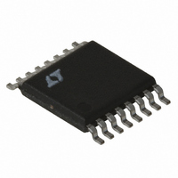
LT1765EFE-5#PBF Linear Technology, LT1765EFE-5#PBF Datasheet - Page 3

LT1765EFE-5#PBF
Manufacturer Part Number
LT1765EFE-5#PBF
Description
IC REG SW STEPDOWN 3A 16-TSSOP
Manufacturer
Linear Technology
Type
Step-Down (Buck)r
Datasheet
1.LT1765ES8PBF.pdf
(20 pages)
Specifications of LT1765EFE-5#PBF
Internal Switch(s)
Yes
Synchronous Rectifier
No
Number Of Outputs
1
Voltage - Output
5V
Current - Output
3A
Frequency - Switching
1.25MHz
Voltage - Input
3 ~ 25 V
Operating Temperature
-40°C ~ 125°C
Mounting Type
Surface Mount
Package / Case
16-TSSOP Exposed Pad, 16-eTSSOP, 16-HTSSOP
Primary Input Voltage
15V
No. Of Outputs
1
Output Voltage
5V
Output Current
6A
No. Of Pins
16
Operating Temperature Range
-40°C To +125°C
Msl
MSL 1 - Unlimited
Supply Voltage Range
3V To 25V
Rohs Compliant
Yes
Lead Free Status / RoHS Status
Lead free / RoHS Compliant
Power - Output
-
Available stocks
Company
Part Number
Manufacturer
Quantity
Price
ELECTRICAL CHARACTERISTICS
The
V
PARAMETER
Maximum Switch Current Limit
Oscillator Frequency
Switch On Voltage Drop
V
V
Shutdown Supply Current
Feedback Voltage
FB Input Current
FB Input Resistance
FB Error Amp Voltage Gain
FB Error Amp Transconductance
V
V
V
V
V
Maximum Switch Duty Cycle
Minimum Boost Voltage Above Switch
Boost Current
SHDN Threshold Voltage
SHDN Threshold Current Hysteresis
SHDN Input Current (Shutting Down)
SYNC Threshold Voltage
SYNC Input Frequency
SYNC Pin Resistance
Note 1: Stresses beyond those listed under Absolute Maximum Ratings
may cause permanent damage to the device. Exposure to any Absolute
Maximum Rating condition for extended periods may affect device
reliability and lifetime.
Note 2: The LT1765E is guaranteed to meet performance specifi cations
from 0°C to 125°C. Specifi cations over the –40°C to 125°C operating
junction temperature range are assured by design, characterization and
correlation with statistical process controls.
IN
IN
C
C
C
C
C
IN
Pin Source Current
Pin Sink Current
Pin to Switch Current Transconductance
Pin Minimum Switching Threshold
Pin 3A ISW Threshold
Undervoltage Lockout
Supply Current
= 15V, V
l
denotes the specifi cations which apply over the full operating temperature range, otherwise specifi cations are at T
C
= 0.8V, Boost = V
IN
+ 5V, SHDN, SYNC and switch open unless otherwise noted.
CONDITIONS
3.3V < V
I = 3A
(Note 3)
V
3V < V
(Note 3)
LT1765 (Adj)
LT1765-1.8
LT1765-2.5
LT1765-3.3
LT1765-5
0.4V < V
ΔI
V
V
Duty Cycle = 0%
V
I
I
I
SHDN = 60mV Above Threshold
I
SW
SW
SW
SYNC
SHDN
FB
FB
C
VC
= 1.2V, I
= V
= V
= 3A
= 1A (Note 4)
= 3A (Note 4)
= ±10μA
= 1mA
IN
= 0V, V
NOM
NOM
IN
C
< 25V, 0.4V < V
< 0.9V
< 25V
SW
– 17%
+ 17%
IN
= 800mA, V
= 25V, V
C
SW
< 0.9V
IN
= 0V
= 6V
Note 3: Minimum input voltage is defi ned as the voltage where the internal
regulator enters lockout. Actual minimum input voltage to maintain a
regulated output will depend on output voltage and load current. See
Applications Information.
Note 4: Current fl ows into the BOOST pin only during the on period of the
switch cycle.
LT1765/LT1765-1.8/LT1765-2.5/
LT1765 (Adj)
LT1765-1.8
LT1765-2.5
LT1765-3.3
LT1765-5
LT1765-3.3/LT1765-5
l
l
l
l
l
l
l
l
l
l
l
l
l
l
l
l
l
l
l
l
l
l
l
l
l
1.182
1.176
1.764
3.234
2.47
2.45
10.5
14.7
1.27
MIN
150
500
1.1
4.9
1.6
–7
19
29
80
70
85
80
3
4
–0.25
1.25
27.5
1.33
–10
TYP
270
350
850
120
110
2.6
1.2
1.8
2.5
3.3
0.4
0.9
1.8
1.5
15
15
21
42
90
20
70
20
4
1
5
5
7
1.218
1.224
1.836
3.366
1300
MAX
–0.5
2.73
2.55
1.40
–13
430
160
180
140
1.6
1.3
5.1
2.7
2.2
A
35
55
21
30
39
60
30
10
6
2
= 25°C.
UNITS
μMho
1765fd
3
MHz
MHz
A/V
mV
mA
mA
mA
kΩ
kΩ
kΩ
kΩ
kΩ
μA
μA
μA
μA
μA
μA
μA
%
%
A
V
V
V
V
V
V
V
V
V
V
V
V


