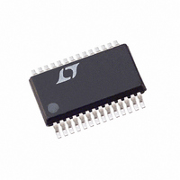
LTC3729EG#PBF Linear Technology, LTC3729EG#PBF Datasheet - Page 11

LTC3729EG#PBF
Manufacturer Part Number
LTC3729EG#PBF
Description
IC SW REG SYNC STEP-DOWN 28-SSOP
Manufacturer
Linear Technology
Series
PolyPhase®r
Type
Step-Down (Buck)r
Datasheet
1.LTC3729EGPBF.pdf
(30 pages)
Specifications of LTC3729EG#PBF
Internal Switch(s)
No
Synchronous Rectifier
Yes
Number Of Outputs
1
Voltage - Output
0.8 ~ 5 V
Current - Output
5A
Frequency - Switching
1.1MHz
Voltage - Input
4 ~ 36 V
Operating Temperature
-40°C ~ 85°C
Mounting Type
Surface Mount
Package / Case
28-SSOP
Primary Input Voltage
36V
No. Of Outputs
1
Output Current
5A
No. Of Pins
28
Operating Temperature Range
-40°C To +85°C
Msl
MSL 1 - Unlimited
Supply Voltage Range
4V To 36V
Rohs Compliant
Yes
Lead Free Status / RoHS Status
Lead free / RoHS Compliant
Power - Output
-
Available stocks
Company
Part Number
Manufacturer
Quantity
Price
OPERATION
INTV
Power for the top and bottom MOSFET drivers and most of
the IC circuitry is derived from INTV
pin is left open, an internal 5V low dropout regulator
supplies INTV
4.7V, the 5V regulator is turned off and an internal switch
is turned on connecting EXTV
the INTV
external source such as the output of the regulator itself
or a secondary winding, as described in the Applications
Information section. An external Schottky diode can be
used to minimize the voltage drop from EXTV
in applications requiring greater than the specified INTV
current. Voltages up to 7V can be applied to EXTV
additional gate drive capability.
Differential Amplifier
This amplifier provides true differential output voltage
sensing. Sensing both V
in high current applications and/or applications having
electrical interconnection losses.
Power Good (PGOOD)
The PGOOD pin is connected to the drain of an internal
MOSFET. The MOSFET turns on when the output is not
within ±7.5% of its nominal output level as determined by
APPLICATIONS INFORMATION
The basic LTC3729 application circuit is shown in Figure 1
on the first page. External component selection is driven
by the load requirement, and begins with the selection
of R
be chosen. Next, the power MOSFETs and D1 and D2 are
selected. The operating frequency and the inductor are
chosen based mainly on the amount of ripple current.
Finally, C
ripple current (that PolyPhase operation minimizes) and
C
ripple voltage and load step specifications (also minimized
with PolyPhase). The circuit shown in Figure 1 can be
configured for operation up to an input voltage of 28V
(limited by the external MOSFETs).
OUT
SENSE1, 2
CC
is chosen with low enough ESR to meet the output
/EXTV
CC
IN
is selected for its ability to handle the input
power to be derived from a high efficiency
. Once R
CC
CC
Power
power. If the EXTV
SENSE1, 2
(Refer to Functional Diagram)
OUT
+
and V
CC
are known, L1 and L2 can
OUT
to INTV
CC
CC
–
. When the EXTV
pin is taken above
benefits regulation
CC
. This allows
CC
to INTV
CC
for
CC
CC
CC
the feedback divider. When the output is within ±7.5% of
its nominal value, the MOSFET is turned off within 10µs
and the PGOOD pin should be pulled up by an external
resistor to a source of up to 7V.
Short-Circuit Detection
The RUN/SS capacitor is used initially to limit the inrush
current from the input power source. Once the controllers
have been given time, as determined by the capacitor on
the RUN/SS pin, to charge up the output capacitors and
provide full load current, the RUN/SS capacitor is then
used as a short‑circuit timeout circuit. If the output volt‑
age falls to less than 70% of its nominal output voltage
the RUN/SS capacitor begins discharging assuming that
the output is in a severe overcurrent and/or short‑circuit
condition. If the condition lasts for a long enough period
as determined by the size of the RUN/SS capacitor, the
controller will be shut down until the RUN/SS pin voltage
is recycled. This built‑in latchoff can be overidden by
providing a >5µA pull‑up current at a compliance of 5V
to the RUN/SS pin. This current shortens the soft‑start
period but also prevents net discharge of the RUN/SS
capacitor during a severe overcurrent and/or short‑circuit
condition. Foldback current limiting is activated when the
output voltage falls below 70% of its nominal level whether
or not the short‑circuit latchoff circuit is enabled.
R
R
rent. The LTC3729 current comparator has a maximum
threshold of 75mV/R
range of SGND to 1.1( INTV
threshold sets the peak inductor current, yielding a maxi‑
mum average output current I
less half the peak‑to‑peak ripple current, ∆I
Allowing a margin for variations in the LTC3729 and external
component values yields:
where N = number of stages.
SENSE
SENSE1, 2
R
SENSE
Selection For Output Current
= (50mV/I
are chosen based on the required output cur‑
MAX
SENSE
)N
and an input common mode
CC
MAX
). The current comparator
equal to the peak value
LTC3729
L
.
11
3729fb


