SC1485ITSTRT Semtech, SC1485ITSTRT Datasheet
SC1485ITSTRT
Specifications of SC1485ITSTRT
Available stocks


Related parts for SC1485ITSTRT


SC1485ITSTRT Summary of contents
Page 1
... TON2 DH2 VOUT2 10 19 VOUT2 LX2 R10 R11 11 18 VCCA2 ILIM2 R12 12 17 FB2 VDDP2 13 16 PGD2 DL2 C10 R14 14 15 VSSA2 PGND2 C12 1uF 1uF VSSA2 1 SC1485 VBAT Q1 C2 10uF L1 VOUT1 VSSA1 VBAT Q3 C8 10uF L2 VOUT2 R13 0R VSSA2 www.semtech.com ...
Page 2
... Notes: (1) This device is ESD sensitive. Use of standard ESD handling precautions is required. (2) Measured in accordance with JESD51-1, JESD51-2 and JESD51-7. Electrical Characteristics Test Conditions 15V, EN/PSV1=EN/PSV2 = 5V, VCCA1 = VDDP1 = VCCA2 = VDDP2 = 5V, V BAT 2005 Semtech Corp. ( > > > SC1485 =1.25V OUT1 OUT2 TON1 TON2 2 ° 5 ...
Page 3
... NOT RECOMMENDED FOR NEW DESIGN POWER MANAGEMENT Electrical Characteristics (Cont.) Test Conditions 15V, EN/PSV1=EN/PSV2 = 5V, VCCA1 = VDDP1 = VCCA2 = VDDP2 = 5V, V BAT 2005 Semtech Corp SC1485 = V =1.25V OUT1 OUT2 TON1 TON2 2 ° ° ° www.semtech.com µ µ µ µ ...
Page 4
... MOSFET. These values guaranteed by the ILIM Source Current and Current Comparator Offset tests. (3) clks = Switching cycles. (4) Guaranteed by design. See Shoot-Through Delay Timing Diagram on Page 6. (5) Semtech’s SmartDriver FET drive first pulls DH high with a pullup resistance of 10 (typ.) until LX = 1.5V (typ.). TM At this point, an additional pullup device is activated, reducing the resistance to 2 (typ ...
Page 5
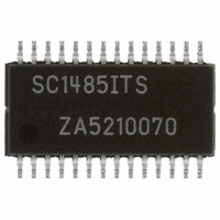
... NOT RECOMMENDED FOR NEW DESIGN POWER MANAGEMENT Pin Configuration TSSOP-28 Pin Descriptions 2005 Semtech Corp. Ordering Information S Notes: (1) Only available in tape and reel packaging. A reel contains 2500 devices. (2) Lead free product. This product is fully WEEE, RoHS and J-STD-020B compliant SC1485 µ ...
Page 6
... NOT RECOMMENDED FOR NEW DESIGN POWER MANAGEMENT Pin Descriptions (Cont Shoot-Through Delay Timing Diagram LX DL tplhDL 2005 Semtech Corp SC1485 µ tplhDH www.semtech.com ...
Page 7
... POR / SS EN/SPV1 (22) TON1 (23) TON VOUT1 (24) TOFF 1.5V REF FB1 (26) X3 PGD1 (27) VSSA1 (28) VCCA2 (11) POR / SS EN/SPV2 (8) TON2 (9) TON VOUT2 (10) TOFF 1.5V REF FB2 (12) X3 PGD2 (13) VSSA2 (14) 2005 Semtech Corp OFF CONTROL LOGIC PWM OC ZERO FAULT UV MONITOR REF + 10% REF - 10% REF - 30 OFF CONTROL LOGIC ...
Page 8
... The SC1485 requires an external +5V bias supply in addition to the battery. If stand-alone capability is required, the +5V supply can be generated with an external linear regulator such as the Semtech LP2951. To avoid interference between outputs, each controller has its own ground reference, VSSA, which should be tied by a single trace to PGND at the negative terminal of that controller’ ...
Page 9
... MOSFET) falls below the voltage across the R resistor. ILIM 2005 Semtech Corp extreme over-current situation, the top MOSFET will never turn back on and eventually the part will latch off due to output undervoltage (see Output Undervoltage Protection). ...
Page 10
... MOSFETs. An adaptive dead-time circuit monitors the DL output and prevents the high-side MOSFET from turning on until DL is fully off (below ~1V). Semtech’s SmartDriver™ FET drive first pulls DH high with a pull-up resistance of 10 (typ.) until LX = 1.5V (typ.). At this ...
Page 11
... For purposes of demonstrating the procedure the output for the schematic in Figure 8 on Page 16 will be designed. 2005 Semtech Corp. The maximum input voltage (V the highest AC adaptor voltage. The minimum input voltage (V ...
Page 12
... VBAT ( MAX ) BAT ( MAX ) OUT For our example 1.74A and I RIPPLE_VBAT(MIN) P-P RIPPLE_VBAT(MAX) 2005 Semtech Corp. From this we can calculate the minimum inductor current rating for normal operation INDUCTOR ( MIN For our example: . The OUT . For our example I ON INDUCTOR(MIN) Next we will calculate the maximum output capacitor = 255ns equivalent series resistance (ESR) ...
Page 13
... Secondly calculating the value of C this TOP TOP C F TOP VBAT ( MIN ) 2005 Semtech Corp. maximum for our For our example we will use 14.3k , therefore: BOT Z = 6.67k TOP We will select a value of C value VBAT ( MIN ) For our example MAX ...
Page 14
... ILIM VALLEY For our example 5.13A and R VALLEY DS(ON) We select the next lowest 1% resistor value: 7.68k 2005 Semtech Corp. Thermal Considerations The junction temperature of the device may be calculated as follows 12m Where ambient temperature (° power dissipation in (W) TOP D = thermal impedance junction to ambient from JA absolute maximum ratings (° ...
Page 15
... NOT RECOMMENDED FOR NEW DESIGN POWER MANAGEMENT gives us 1100 10 5 150 250 300 182 W and 182 84 100 can be seen, the heating effects due to internal power dissipation are practically negligible, thus requiring no special consideration thermally during layout. 2005 Semtech Corp 1875 SC1485 www.semtech.com ...
Page 16
... VOUT VOUT2 C15 R9 20k0 56p 0402 0402 PGOOD R13 C18 20k0 0402 1nF 0402 Figure 8: Reference Design and Layout Example 2005 Semtech Corp. 5VSUS 5VSUS D1 SOD323 U1 SC1485 C5 0.1uF 22 7 EN/PSV1 BST1 0603 23 6 TON1 DH1 24 5 VOUT1 LX1 ...
Page 17
... Connect VSSA1 and VSSA2 using either a wide (>0.020”) trace. Very little current flows in the chip ground therefore large areas of copper are not needed. PGOOD PGOOD Figure 9: Components Connected to VSSA1 and VSSA2 2005 Semtech Corp. VBAT 5VSUS R1 R2 ...
Page 18
... Note that there are two separate traces, one for VSSA1 and one for VSSA2. Decoupling capacitors C9 and C19 are as close as possible to their pins, as are VDDP decoupling capacitors C10 and C20. C10 and C20 should connect to the ground plane using two vias each. 2005 Semtech Corp. Figure 10: Example VSSA 0.020” Traces 18 SC1485 www ...
Page 19
... In Figure 11, VOUT1 and VSSA1 are routed as a differential pair from the output capacitors back to the feedback components and device. Similarly, VOUT2 and VSSA2 are routed as a differential pair from the output capacitors back to the feedback components and device. 2005 Semtech Corp. VOUT1 VSSA1 ...
Page 20
... EMI. Use large copper pours to minimize losses and parasitics. Exactly the same philosophy applies to the OUT1 power section and input loop. Figure 13 below shows an example of the layout for the power section using these guidelines. Figure 13: Power Component Placement and Copper Pours 2005 Semtech Corp. Q3 IRF7811AV 8 1 ...
Page 21
... Phase nodes (black copper islands (preferred) or wide copper traces. Gate drive traces (red) and phase node traces (blue wide copper traces (L:W < 20:1) and as short as possible, with DL the most critical. 2005 Semtech Corp. resistor at the bottom of the output capacitor to connect to VSSA1/2 for ...
Page 22
... V = 20V BAT 200 150 100 (A) OUT Please refer to Figure 8 on Page 16 for test schematic (OUT2) 2005 Semtech Corp. 1.2V Efficiency (Continuous Conduction Mode) vs. Output Current vs. Input Voltage 100 1.2V Output Voltage (Continuous Conduction Mode) vs. Output Current vs. Input Voltage 1 ...
Page 23
... Load Transient Response, Continuous Conduction Mode Zoomed Load Transient Response, Continuous Conduction Mode Zoomed Please refer to Figure 8 on Page 16 for test schematic (OUT2) 2005 Semtech Corp. Trace 1: 1.2V, 50mV/div., AC coupled Trace 2: LX, 20V/div Trace 3: not connected Trace 4: load current, 5A/div Timebase: 40µs/div. ...
Page 24
... Load Transient Response, Power Save Mode Zoomed Load Transient Response, Power Save Mode Zoomed Please refer to Figure 8 on Page 16 for test schematic (OUT2) 2005 Semtech Corp. Trace 1: 1.2V, 50mV/div., AC coupled Trace 2: LX, 20V/div Trace 3: not connected Trace 4: load current, 5A/div Timebase: 40µs/div. ...
Page 25
... POWER MANAGEMENT Typical Characteristics (Cont.) Startup (PSV), EN/PSV Going High Startup (CCM), EN/PSV 0V to Floating Please refer to Figure 8 on Page 16 for test schematic (OUT2) 2005 Semtech Corp. Trace 1: 1.2V, 0.5V/div. Trace 2: LX, 10V/div Trace 3: EN/PSV, 5V/div Trace 4: PGD, 5V/div. Timebase: 1ms/div. ...
Page 26
... N/2 TIPS aaa C SEATING PLANE C SIDE VIEW NOTES: 1. CONTROLLING DIMENSIONS ARE IN MILLIMETERS (ANGLES IN DEGREES). 2. DATUMS -A- AND -B- 3. DIMENSIONS "E1" AND "D" DO NOT INCLUDE MOLD FLASH, PROTRUSIONS OR GATE BURRS. 4. REFERENCE JEDEC STD MO-153, VARIATION AE. 2005 Semtech Corp. DIM e aaa bbb ccc ...
Page 27
... POWER MANAGEMENT Land Pattern - TSSOP-28 X (C) P NOTES: 1. THIS LAND PATTERN IS FOR REFERENCE PURPOSES ONLY. CONSULT YOUR MANUFACTURING GROUP TO ENSURE YOUR COMPANY'S MANUFACTURING GUIDELINES ARE MET. Contact Information Phone: (805)498-2111 FAX (805)498-3804 2005 Semtech Corp. DIM Semtech Corporation Power Management Products Division ...