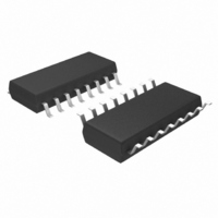
MIC2182-5.0YM Micrel Inc, MIC2182-5.0YM Datasheet - Page 13

MIC2182-5.0YM
Manufacturer Part Number
MIC2182-5.0YM
Description
IC CTRLR SYNC BUCK 5.0V 16-SOIC
Manufacturer
Micrel Inc
Type
Step-Down (Buck)r
Datasheet
1.MIC2182-5.0YSM.pdf
(28 pages)
Specifications of MIC2182-5.0YM
Internal Switch(s)
No
Synchronous Rectifier
Yes
Number Of Outputs
1
Voltage - Output
5V
Current - Output
20A
Frequency - Switching
300kHz
Voltage - Input
4.5 ~ 16.5 V
Operating Temperature
-40°C ~ 85°C
Mounting Type
Surface Mount
Package / Case
16-SOIC (3.9mm Width)
Power - Output
400mW
Lead Free Status / RoHS Status
Lead free / RoHS Compliant
Other names
576-2158
MIC2182-5.0YM
MIC2182-5.0YM
Available stocks
Company
Part Number
Manufacturer
Quantity
Price
Company:
Part Number:
MIC2182-5.0YM
Manufacturer:
MICREL
Quantity:
48
Company:
Part Number:
MIC2182-5.0YM
Manufacturer:
MICREL
Quantity:
784
Part Number:
MIC2182-5.0YM
Manufacturer:
MICREL/麦瑞
Quantity:
20 000
Switching from PWM to Skip Mode
The current sense amplifier in Figure 3 monitors the average
voltage across the current-sense resistor. The controller will
switch from PWM to skip mode when the average voltage
across the current-sense resistor drops below approximately
12mV. This is shown in Figure 7b. The average output current
at this transition level for is calculated below.
where:
Switching from Skip to PWM Mode
The frequency of occurrence of the skip-mode current pulses
increase as the output current increases until the hysteretic
duty cycle reaches 100% (continuous pulses). Increasing the
current past this point will cause the output voltage will drop.
The low limit comparator senses the output voltage when it
drops below 2% of the set output and automatically switches
the converter to PWM mode.
The inductor current in skip mode is a triangular wave shape
a minimum value of 0 and a maximum value of 35mV/R
(see Figure 7b). The maximum average output current in skip
mode is the average value of the inductor waveform:
The capacitor on the PWM pin (pin 2) is discharged when the
IC transitions from skip to PWM mode. This forces the IC to
remain in PWM mode for a fixed period of time. The added
delay prevents unwanted switching between PWM and skip
mode. The capacitor is charged with a 10uA current source
on pin 2. The threshold on pin 2 is 2.5V. The delay for a typical
1nF capacitor is:
where:
Current Limit
The current-limit circuit operates during PWM mode. The
output current is detected by the voltage drop across the
external current-sense resistor (R
April 22, 2004
MIC2182
0.012 = threshold voltage of the internal comparator
R
C
I
I
t
OUT(skipmode)
OUT(max skipmode)
delay
CS
PWM
Inductor
= current-sense resistor value
Current
Inductor
= capacitor connected to pin 2
Current
C
PWM
I
source
Figure 7b. Minimum PWM-Mode-Load Inductor Current for PWM Operation
I
0.012
V
MIN(PWM)
R
threshold
I
CS
LIM(skip)
0.5
0A
0A
35mV
Figure 7a. Maximum Skip-Mode-Load Inductor Current
R
CS
CS
1nF 2.5V
10 A
in Figure 2.). The cur-
250 s
CS
13
rent-limit threshold is 100mV+35mV –25mV. The current-
sense resistor must be sized using the minimum current-limit
threshold. The external components must be designed to
withstand the maximum current limit. The current-sense
resistor value is calculated by the equation below:
The maximum output current is:
The current-sense pins CSH (pin 8) and V
noise sensitive due to the low signal level and high input
impedance. The PCB traces should be short and routed close
to each other. A small (1nF to 0.1 F) capacitor across the pins
will attenuate high frequency switching noise.
When the peak inductor current exceeds the current-limit
threshold, the current-limit comparator, in Figure 2, turns off
the high-side MOSFET for the remainder of the cycle. The
output voltage drops as additional load current is pulled from
the converter. When the output voltage reaches approxi-
mately 0.95V, the circuit enters frequency-foldback mode
and the oscillator frequency will drop to 60kHz while maintain-
ing the peak inductor current equal to the nominal 100mV
across the external current-sense resistor. This limits the
maximum output power delivered to the load under a short
circuit condition.
Reference, Enable, and UVLO Circuits
The output drivers are enabled when the following conditions
are satisfied:
The internal bias circuit generates a 1.245V bandgap refer-
ence voltage for the voltage error amplifier and a 5V V
voltage for the gate drive circuit. The reference voltage in the
fixed-output-voltage versions of the MIC2182 is buffered and
brought to pin 7. The V
(pin 4) with a 0.1 F capacitor. The adjustable version of the
MIC2182 uses pin 7 for output voltage sensing. A decoupling
capacitor on pin 7 is not used in the adjustable output voltage
version.
• The V
• The voltage on the enable pin is greater than the
R
I
OUT(max)
undervoltage threshold (typically 4.2V).
enable UVLO threshold (typically 2.5V)
CS
DD
I
OUT(max)
75mV
voltage (pin 11) is greater than its
135mV
R
CS
REF
pin should be bypassed to GND
12mV THRESHOLD
OF AVERAGE VOLTAGE
ACROSS R
35mV THRESHOLD
ACROSS R
CS
.
CS
.
OUT
M9999-042204
(pin 9) are
Micrel
DD


