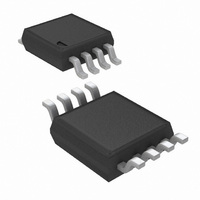
LM3489MM/NOPB National Semiconductor, LM3489MM/NOPB Datasheet

LM3489MM/NOPB
Specifications of LM3489MM/NOPB
LM3489MMTR
Available stocks
Related parts for LM3489MM/NOPB
LM3489MM/NOPB Summary of contents
Page 1
... No control loop compensation required ■ Wide 4.5V to 35V input range ■ 1.239V to V adjustable output range IN Typical Application Circuit © 2008 National Semiconductor Corporation ■ High efficiency 93% ■ ±1.3% (±2% over temp) internal reference ■ 100% duty cycle operation ■ Maximum operation frequency > 1MHz ■ ...
Page 2
Connection Diagram Package Marking and Ordering Information Order Number Package Type LM3489MM MSOP-8 LM3489MMX MSOP-8 LM3489QMM MSOP-8 LM3489QMMX MSOP-8 *Automotive Grade (Q) product incorporates enhanced manufacturing and support processes for the automotive market, including defect detection methodologies. Reliability qualification is ...
Page 3
... Absolute Maximum Ratings If Military/Aerospace specified devices are required, please contact the National Semiconductor Sales Office/ Distributors for availability and specifications. VIN Voltage PGATE Voltage FB Voltage ISENSE Voltage ADJ Voltage EN Voltage (Note 3) Maximum Junction Temp. Power Dissipation 25°C (Note A 2) Electrical Characteristics ...
Page 4
Note 1: Absolute maximum ratings are limits beyond which damage to the device may occur. Operating Ratings are conditions for which the device is intended to be functional, but device parameter specifications may not be guaranteed. For guaranteed specifications and ...
Page 5
Feedback Voltage Hysteresis vs Temperature Current Limit One Shot OFF Time vs. Temperature Minimum ON Time vs Temperature (Normal Operation) Current Limit ADJ Current vs Temperature 20186905 V IN 20186907 Minimum ON Time vs Temperature (Current Limit) 20186941 5 20186906 ...
Page 6
Operating ON Time vs Load Current Efficiency vs Load Current (V = 3.3V 22µH) OUT Efficiency vs Load Current ( 22µH) OUT www.national.com Operating Frequency vs Input Voltage 20186911 V Regulation vs Load Current ...
Page 7
Power Up (No Load 1nF) ADJ 20186957 Discontinuous Mode Operation (V = 12V 50mA) IN OUT OUT 20186951 Enable Transient (V = 3.3 V, 500 mA Loaded) OUT 20186955 Continuous Mode Operation (V ...
Page 8
Simplified Functional Block Diagram Functional Description OVERVIEW The LM3489 is a buck (step-down) DC-DC controller that us hysteretic control scheme. The control comparator is designed with approximately 10mV of hysteresis. In response to the voltage at the FB ...
Page 9
( OUT_PP HYST For example, with V set to 3.3V, V OUT OUT_PP V = 0.01 x (33K + 20k) / 20k = 0.0266V OUT_PP Operating frequency (F) is determined by knowing the ...
Page 10
FIGURE 4. Current Limit Fold Back Phenomenon At high input voltages (>28V) increased undershoot at the switch node can cause an increase in the current limit thresh- old. To avoid this problem, a low Vf Schottky catch diode must be ...
Page 11
V is the enable rising threshold voltage and the enable threshold hysteresis. EN_HYST Design Information Hysteretic control is a simple control scheme. However the operating frequency and other performance characteristics highly depend on external conditions and ...
Page 12
The input capacitor power dissipation can be calculated as follows ESR D(CIN) RMS_CIN The input capacitor must be able to handle the RMS current and the dissipation. Several input capacitors may be con- nected in ...
Page 13
PCB Layout The PCB board layout is very important in all switching regu- lator designs. Poor layout can cause switching noise into the feedback signal and generate EMI problems. For minimal in- ductance, the wires indicated by heavy lines in ...
Page 14
Physical Dimensions www.national.com inches (millimeters) unless otherwise noted 8 Lead Plastic MSOP-8 NS package Number MUA08A 14 ...
Page 15
Notes 15 www.national.com ...
Page 16
... For more National Semiconductor product information and proven design tools, visit the following Web sites at: Products Amplifiers www.national.com/amplifiers Audio www.national.com/audio Clock Conditioners www.national.com/timing Data Converters www.national.com/adc Displays www.national.com/displays Ethernet www.national.com/ethernet Interface www.national.com/interface LVDS www.national.com/lvds Power Management www.national.com/power Switching Regulators www.national.com/switchers LDOs www ...


